System and method for capturing and positioning particles

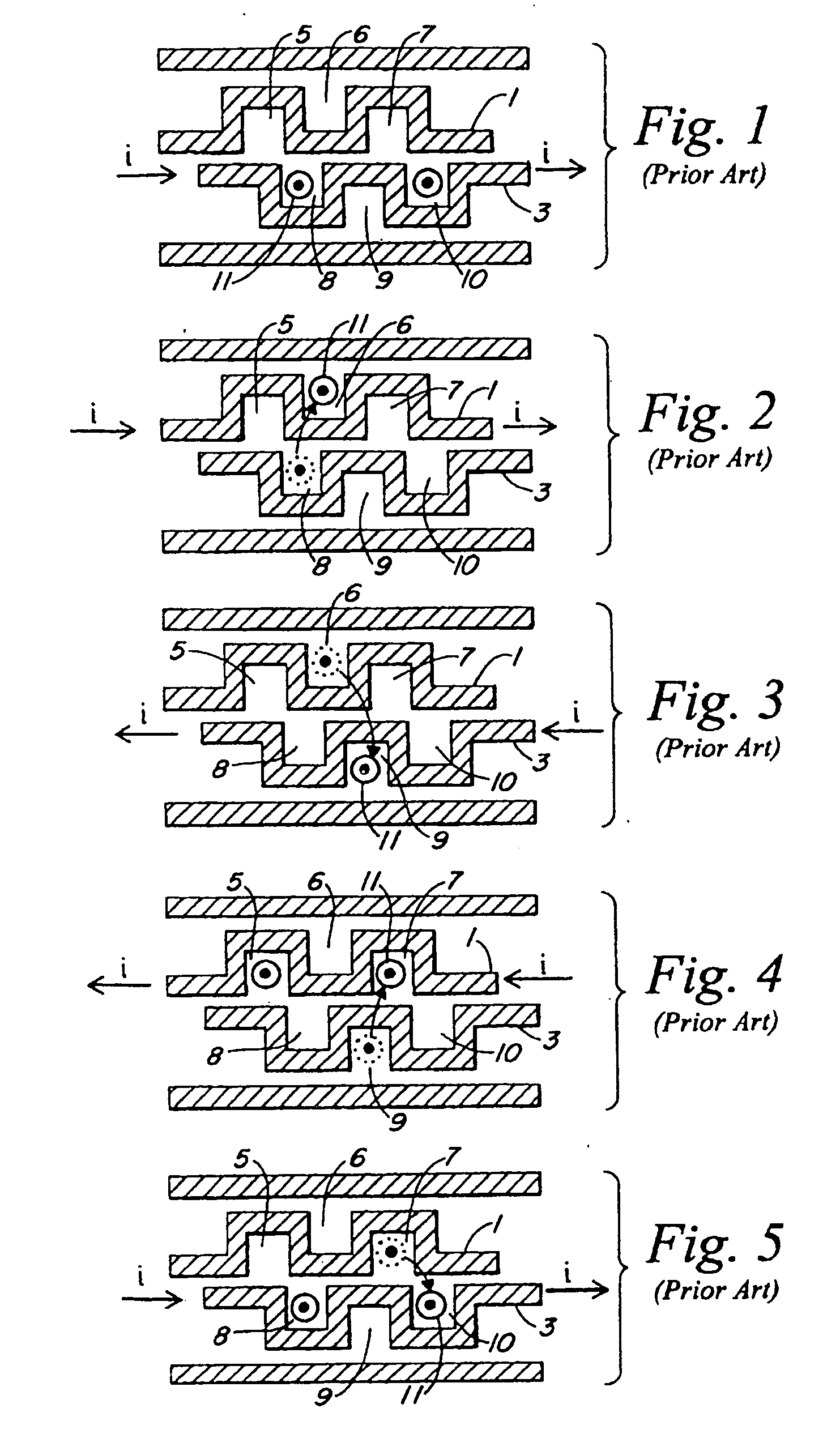
a technology of positioning and particle, applied in the field of nanoscale object control, can solve the problems of limited number of traps that can be simultaneously formed and independently controlled, and the tip of two or more scanning probe electromagnet tweezers cannot be close together, and the conventional magnetic tweezers fail to provide individual control of multiple magnetic beads

Inactive Publication Date: 2004-12-30
PRESIDENT & FELLOWS OF HARVARD COLLEGE
View PDF5 Cites 78 Cited by
  • Summary
  • Abstract
  • Description
  • Claims
  • Application Information

AI Technical Summary

Benefits of technology

0039] Another aspect of the present invention is an integrated circuit for capturing and positioning particles. The integrated circuit includes an access window; a plurality of individually addressable microconductors located in the access window, the plurality of individually addressable microconductors having different directions and forming in a matrix; and a micro-controller to control an amount of voltage being applied to each of the individually addressable microconductors.
0040] A further aspect of the present invention is an integrated circuit for capturing and positioning particles. The integrated circuit includes an access window; a plurality of individually addressable microconductors located in the access window, the plurality of individually addressable microconductors having different directions and forming in a matrix; and a micro-controller to control an amount of current or voltage being applied to each of the individually addressable microconductors.

Problems solved by technology

However, conventional magnetic tweezers fail to provide individual control of multiple magnetic beads because conventional magnetic beads can only control one bead or group of beads, not many beads individually
However, since the scanning probe electromagnet tip is cone shaped and it is attached to a larger cantilever, it is very difficult to operate two or more scanning probe electromagnet tweezers simultaneously with the tips close together.
However, the number of traps that can be simultaneously formed and independently controlled is limited since each trap needs a focused laser beam with the appropriate scanning instruments.
The dielectrophoresis traps, which have been realized so far, are good at trapping many neutral particles simultaneously but their capabilities of moving trapped particles are still limited.
However, the conventional device of FIGS. 1-5 cannot independently move separate groups of magnetic particles.
In all the conventional devices and methods described above, small particles can be separated or trapped in a liquid, fluid, or other type of environment using magnetic or electric fields; however, these conventional devices cannot produce a number of peaks in magnetic or electric field amplitude that can be independently controlled at different positions with nanoscale resolution.
Moreover, these conventional devices cannot provide movement of particles suspended in a fluid with nanoscale resolution at room temperature.

Method used


Image

  • System and method for capturing and positioning particles
  • System and method for capturing and positioning particles
  • System and method for capturing and positioning particles

Examples


example 1

[0108] 1. Substrate cleaning (TCE, Acetone, and Methanol)

[0109] 2. Photolithography (1.sup.st microconductor conductor array pattern)

1 Spin Primer 5000 rpm 40 sec Spin Photoresist 1813 5000 rpm 40 sec Bake(hot plate) substrate 100.degree. C. 3 min 30 sec UV exposure 10 mW / cm.sup.2 6 sec Evaporate Cr 100 .ANG. Au 800 .ANG.

[0110] 3. Plate with gold solution

[0111] Attach leads to the Au pattern in the substrate

[0112] Put the sample and electrode(Pt) in Au solution

[0113] Sample-cathode(-)

[0114] Pt plate-anode(+)

[0115] Apply current (0.1 mA) until the resistance of the pattern drops to 100 .OMEGA.

[0116] 4. Photosensitive polyimide (1.sup.st insulating layer)

2 Spin HD2729 6000 rpm 45 sec Soft bake(hot plate) 60.degree. C. 4 min 80.degree. C. 4 min 100.degree. C. 4 min Contact pads mask UV exposure 10 mW / / cm.sup.2 1 min Develop in DE 6180 40 s Rinse in RI 9180 20 s Blow dry 20 s Thermal cure(hot plate) 120.degree. C. 30 min ramp up to 260.degree. C. at 2.degree. C. / min, 260.degree. C. 30 m...

example 2

[0124] 1. Clean Silicon wafers: Ultrasonic 10 min. each in TCE, Acetone and Methanol and blow dry.

[0125] 2. Spin PMMA (495K, 4%)

4 a. 500 rpm 5 sec b. 3000 rpm 30 sec

[0126] 3. Softbake(on hot plate) 5 min at 180 C.

[0127] 4. Spin PMMA (495K, 4%)

5 a. 500 rpm 5 sec b. 3000 rpm 30 sec

[0128] 5. Softbake(on hot plate) 5 min at 180 C.

[0129] 6. Spin PMMA (950K, 2%)

6 a. 500 rpm 5 sec b. 3000 rpm 40 sec

[0130] 7. Softbake(on hot plate) 5 min at 180 C.

[0131] 8. Write the patterns of the 1.sup.st layer microconductor array using E-beam lithography

[0132] 9. Develop the patterns using PMMA developer (1 min)

[0133] 10. Evaporate Cr (10 nm) and Au (200 nm) using thermal evaporator.

[0134] 11. Lift off: Removes unexposed parts.

[0135] 12. Evaporate Al.sub.3O.sub.4 for 200 nm: acts as an insulator

[0136] 13. Repeat 2-12: writing second layer of conductors and insulator

[0137] 14. Attach the leads

[0138] The choice of substrate on which the matrix is fabricated preferably is made based on three major factors:...


PUM

PropertyMeasurementUnit
widthaaaaaaaaaa
diameteraaaaaaaaaa
heightaaaaaaaaaa

Abstract

A micro-electromagnet matrix captures and controls the movement of particles with nanoscale resolution. The micro-electromagnet matrix includes multiple layers of microconductors, each layer of microconductors being orthogonal to an adjacent layer or microconductors. The layers of microconductors are formed on a substrate and have insulating layers therebetween. The field patterns produced by the micro-electromagnet matrix enable precise manipulation of particles. The micro-electro-magnet matrix produces single or multiple independent field peaks in the magnetic field that are used to trap, move, or rotate the particles. The micro-electromagnet matrix also produces electromagnetic fields to probe and detect particles.

Description

CROSS-REFERENCE TO RELATED PROVISIONAL APPLICATION[0001] The present patent application claims priority under 35 U.S.C. .sctn.119 from U.S. Provisional Patent Application Ser. No. 60 / 338,236 filed on Nov. 5, 2001. The entire contents of U.S. Provisional Patent Application Ser. No. 60 / 338,236 filed on Nov. 5, 2001 are hereby incorporated by reference.FIELD OF THE PRESENT INVENTION[0002] The present invention is directed to controlling the position of nanoscale objects. More specifically, the present invention is directed to the generation of magnetic or electric fields that are used to trap, move, rotate, probe, detect, study, manipulate, and / or magnetic resonance image particles with nanoscale resolution.BACKGROUND OF THE PRESENT INVENTION[0003] Interests in study and manipulation of nanoscale magnetic particles or nanoscale semiconductor particles have grown significantly with the advances in particle synthesis. Because of their small size, these particles show quantum characterist...

Claims


Application Information

Patent Timeline
Patent Type & Authority Applications(United States)
IPC IPC(8): B01L3/00B03C1/24G01N15/14
CPCB01L3/502761B01L3/502792B01L2200/0647B01L2200/0668B01L2300/089B01L2400/0415B01L2400/043B03C1/24B03C2201/22G01N15/1456
Inventor WESTERVELT, ROBERT M.LEE, CHUNGSOKLEE, HAKHO
Owner PRESIDENT & FELLOWS OF HARVARD COLLEGE
Why Eureka
Try Eureka