Electro-optical device and electronic apparatus

a technology of optical devices and electronic devices, applied in the direction of static indicating devices, instruments, doors, etc., can solve the problems of low luminous efficiency of light-emitting elements, rapid deterioration of current-luminance characteristics of oleds, and particularly inferior luminous efficiency of oleds, so as to prevent heat drift, reduce the propagation of heat to transistors, and reliably attenuate the

Active Publication Date: 2005-01-06
SEIKO EPSON CORP
View PDF4 Cites 37 Cited by
  • Summary
  • Abstract
  • Description
  • Claims
  • Application Information

AI Technical Summary

Benefits of technology

[0012] Furthermore, in the electro-optical device, the distance between each heat-release section and the electrode connected to the driving circuit is greater than or equal to the thickness of an insulating layer disposed between the light-emitting elements and the heat-release sections and is less than or equal to the pitch between the pixel regions. The insulating layer disposed between the light-emitting elements and the heat-release sections corresponds to a gate insulating layer, an interlayer insulating layer, or the like when the driving circuit includes a thin-film transistor. According to such a configuration, heat can be released from the light-emitting elements to the heat-release sections before the heat causes negative effects on the transistors. Therefore, heat drift can be prevented from affecting the transistors. Hence, the electro-optical device does not depend on temperature changes.
[0013] In the electro-optical device, the heat-release sections have a thermal conductivity greater than or equal to that of a first electrode that is one of a plurality of electrodes connected to the light-emitting elements and has the highest thermal conductivity. In order to obtain such a configuration, the heat-release sections may have a thickness greater than that of the first electrode or a thermal conductivity greater than that of the first electrode. Since the heat-release sections have a thermal conductivity greater than or equal to that of the first electrode having the highest thermal conductivity, heat can be efficiently released from the light-emitting elements to the heat-release sections; hence, the electro-optical device has high heat resistance.
[0015] Since the pixel regions include heat-conductive sections, heat generated from the light-emitting element can be efficiently transmitted to the heat-release sections and temporarily stored in the heat-conductive sections uniformly. Therefore, the temperature distribution in the pixel regions is uniform and the luminance of the light-emitting elements in the pixel regions is uniform; hence, the electro-optical device displays a uniform image.
[0017] In the electro-optical device, the heat-conductive sections are each disposed between the corresponding driving circuits and the corresponding light-emitting elements and each include corresponding third heat-conductive layers located on the side close to the driving circuits, and the third heat-conductive layers have a thermal conductivity less than that of the first heat-conductive layers. According to such a configuration, the propagation of heat to the transistors can be minimized and heat drift can therefore be prevented from affecting the transistors; hence, the electro-optical device does not depend on temperature changes.
[0018] In the electro-optical device, the heat-release sections or the heat-conductive sections are each disposed between the corresponding driving circuits and the corresponding light-emitting elements and function as portions of light-shielding section for shielding the driving circuits from light emitted from the light-emitting elements. Furthermore, the heat-release sections have faces facing the light-emitting elements and the faces or the second heat-conductive layers absorb at least light. The electro-optical device may further include partitions, disposed above the driving circuits, for isolating the luminous sections from each other. The partitions have faces fronting in the light-withdrawing direction and the faces absorb at least light. The distance between the driving circuits and luminous portions of the light-emitting elements is preferably greater than or equal to the distance between the partitions and the heat-release sections or the heat-conductive sections and less than or equal to the pitch between the pixels. According to such a configuration, light entering the transistors can be reliably attenuated. Hence, the electro-optical device has high reproducibility in tone properties.
[0019] When an electronic apparatus includes the electro-optical device described above, the electronic apparatus has high display performance. Hence, the sales appeal of the apparatus can be enhanced.

Problems solved by technology

In general, light-emitting elements are low in luminous efficiency, and OLEDs are particularly inferior in luminous efficiency and convert received energy into heat.
Since current-luminance characteristics of the OLEDs are rapidly deteriorated due to heat generated therefrom during light emission, the display performance of electro-optical devices including the OLEDs cannot be maintained.
Furthermore, since emitted light enters channel regions of thin-film transistors for controlling gradation or retaining image signals, tone reproducibility cannot be satisfactorily maintained.
In particular, when the light-emitting elements include OLEDs including light-emitting layers containing an organic material and the heat-release sections that have a large thickness so as to efficiently transmit the heat are placed above the OLEDs, stress is applied to the OLEDs from the heat-release sections; hence, the OLEDs are deteriorated.

Method used


Image

  • Electro-optical device and electronic apparatus
  • Electro-optical device and electronic apparatus
  • Electro-optical device and electronic apparatus

Examples


Embodiment Construction

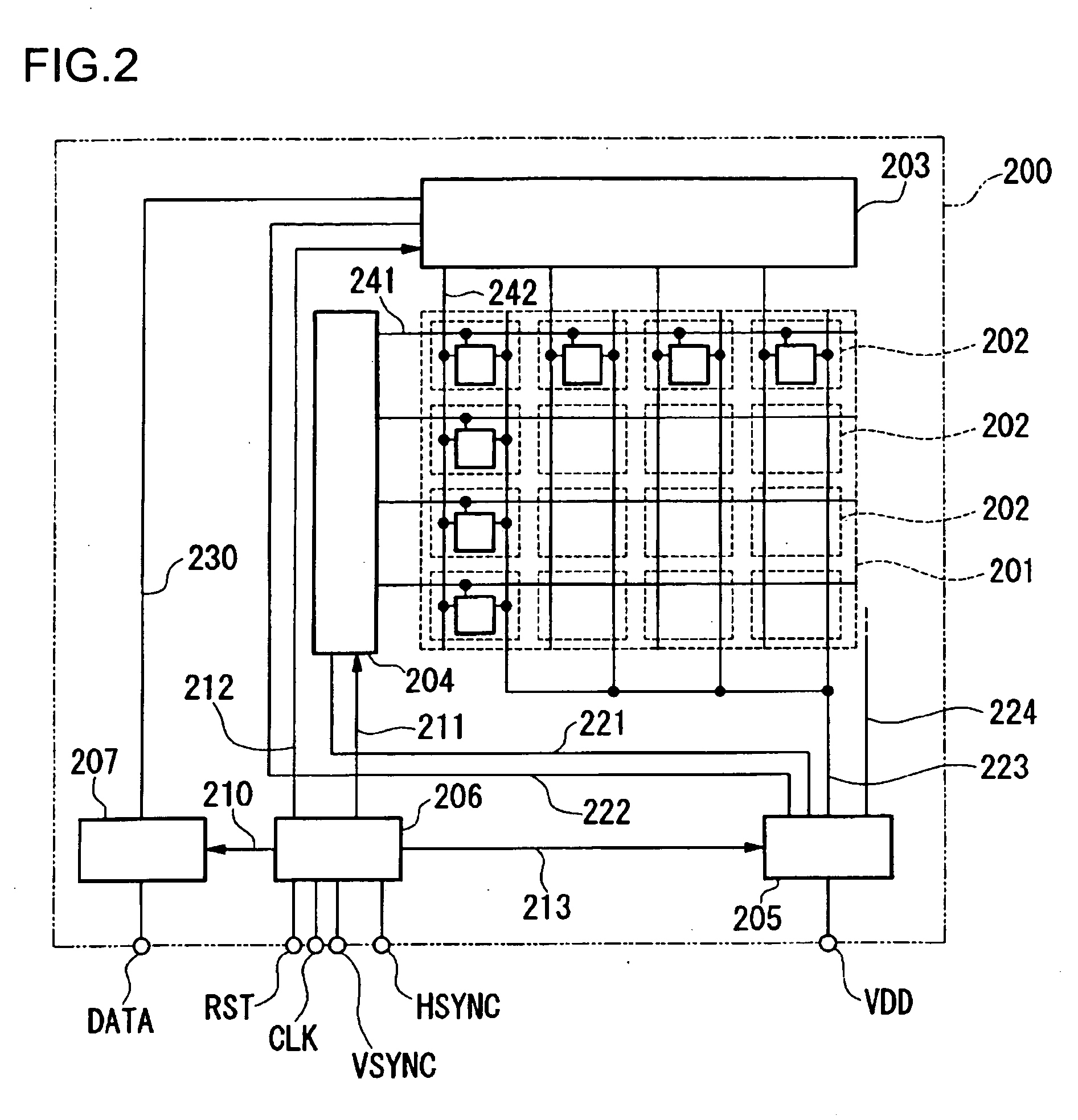
[0027]FIG. 2 is an illustration showing a configuration of an electro-optical device according to an embodiment of the invention, the electro-optical device being an organic electroluminescent (EL) device in particular. FIG. 3 is an illustration showing a configuration of one of active matrix pixels placed in the electro-optical device of this embodiment. The electro-optical device will now be described with reference to FIGS. 2 and 3.

[0028] The electro-optical device 200 has an effective viewing area 201 including a plurality of pixel regions 202 arranged in a matrix. The electro-optical device 200 further includes a plurality of gate wires 241 and source wires 242, intersecting each other, for applying arbitrary image signals to the pixel regions 202. The pixel regions 202 are coupled to each other and arranged depending on the intersections. The pixel regions 202 each include corresponding OLEDs 301 and pixel-driving circuits for each driving the corresponding OLEDs 301. A gate ...


PUM


Abstract

The invention provides an electro-optical device that can include a plurality of scanning lines, a plurality of signal lines, a plurality of pixels arranged corresponding to intersections of the scanning lines and the signal lines, and heat-release sections. The pixels can each include corresponding transistors and corresponding light-emitting elements, the light-emitting elements emit light in the direction that light is withdrawn, and the heat-release sections include heat release portions, located on the side opposite to the light-withdrawing direction of the light-emitting elements, having electrical conductivity. Accordingly, the invention can enhance the environmental resistance of an electro-optical device including light-emitting elements.

Description

BACKGROUND OF THE INVENTION [0001] 1. Field of Invention [0002] The present invention relates to electro-optical devices and electronic apparatuses. The invention particularly relates to an electro-optical device including a light-emitting element having high heat resistance and light resistance and also relates to an electronic apparatus. [0003] 2. Description of Related Art [0004] In recent years, displays including OLEDs (organic light-emitting diodes) functioning as display elements have been attracting much attention. The OLEDs belong to the category of a current-driven light-emitting diode that emits light depending on a current flowing in the diode. In order to display an image using the OLEDs arranged in a matrix, active matrix addressing is used. [0005] For example, PCT Japanese Translation Patent Publication No. WO98 / 12689 discloses an active element, including a polysilicon thin-film transistor, for active matrix addressing. A report (J. Kanicki, J. H. Kim (Univ. of Michi...

Claims


Application Information

Patent Timeline
Patent Type & Authority Applications(United States)
IPC IPC(8): G09G3/30H05B33/02H01L27/32H01L31/062H01L51/50H01L51/52H05B33/14H05B33/26
CPCH01L27/3223H01L2251/558H01L51/529H01L27/3244H10K59/88H10K59/12H10K50/87H10K2102/351B60J5/0498B60J5/0494B60Y2200/145
Inventor OZAWA, TOKUROIMAMURA, YOICHIKASAI, TOSHIYUKI
Owner SEIKO EPSON CORP
Why Eureka
Try Eureka