Intergrated semiconductor component for high-frequency measurement and use thereof

a technology of intergrated semiconductors and high-frequency measurement, which is applied in the direction of instruments, resonant antennas, and using reradiation, etc., can solve the problems of inability to arbitrarily miniaturize, the laser distance meters are substantially more precise, and the relative imprecise is not very precis

Inactive Publication Date: 2005-01-06
ROBERT BOSCH GMBH
View PDF11 Cites 7 Cited by
  • Summary
  • Abstract
  • Description
  • Claims
  • Application Information

AI Technical Summary

Problems solved by technology

Ultrasound instruments are very economical, but because the beam is not sharply focused they are relatively imprecise.
Laser distance meters are substantially more-precise, but cannot be miniaturized arbitrarily and are very expensive.
A disadvantage of this is

Method used


Image

  • Intergrated semiconductor component for high-frequency measurement and use thereof
  • Intergrated semiconductor component for high-frequency measurement and use thereof
  • Intergrated semiconductor component for high-frequency measurement and use thereof

Examples


Embodiment Construction

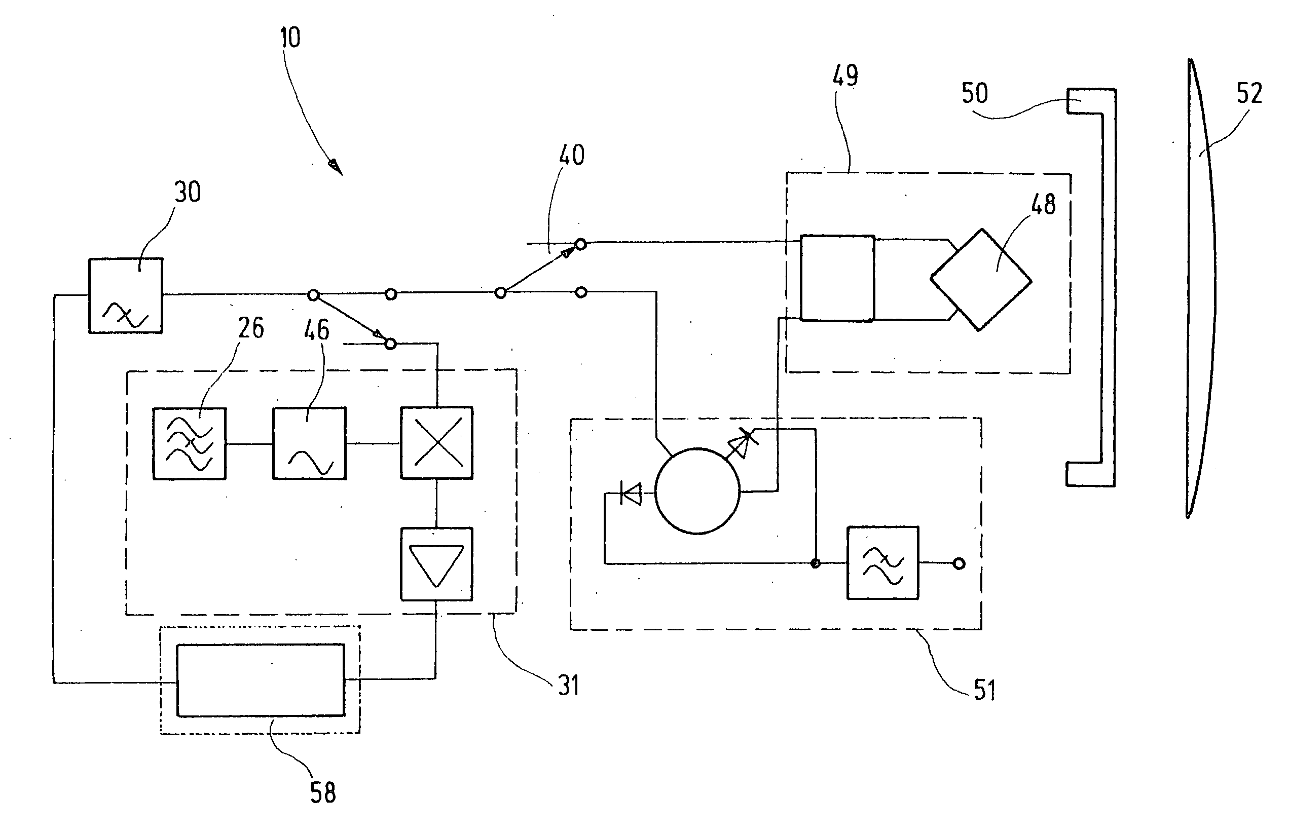
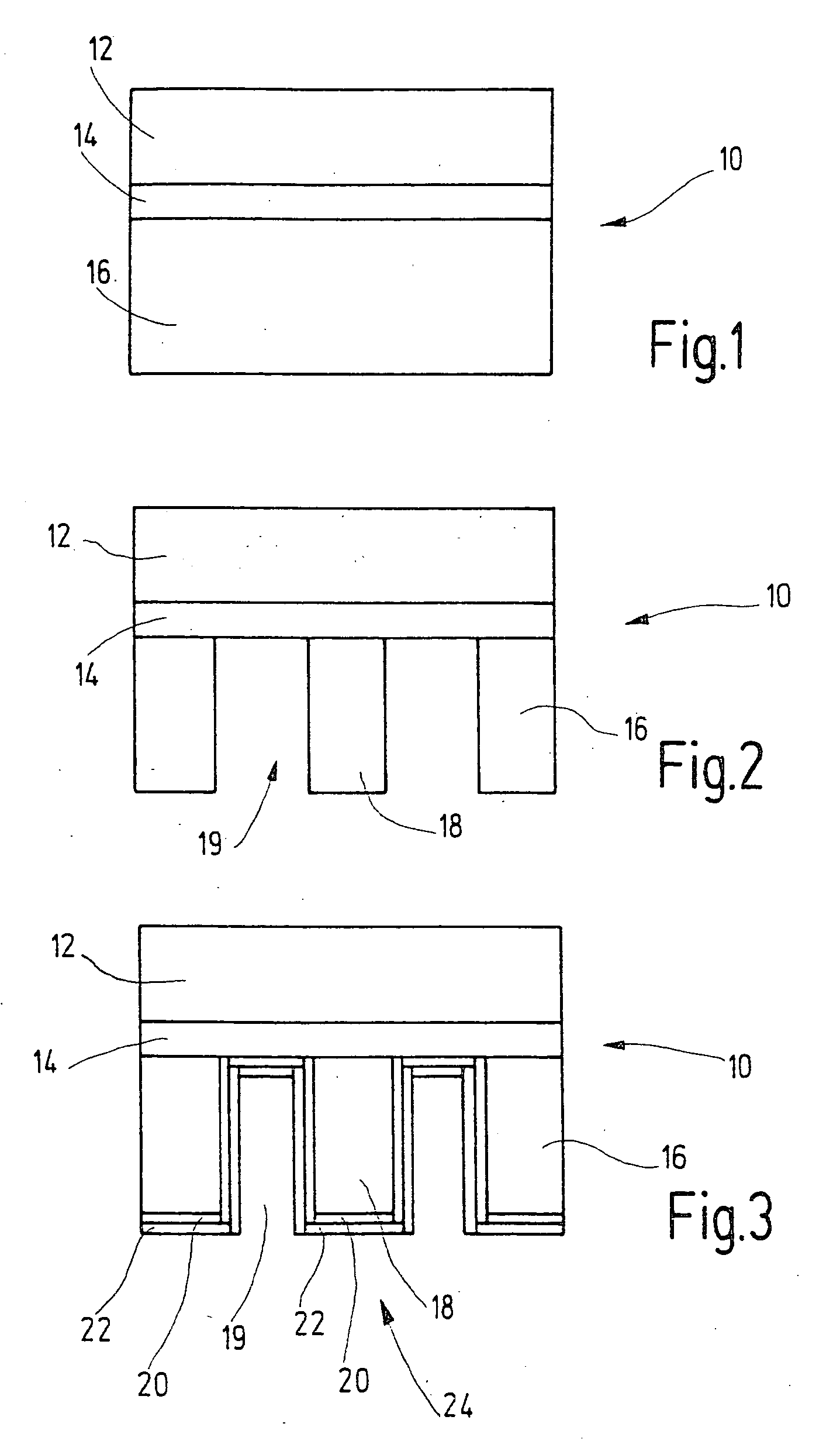
[0029]FIG. 1, in a schematic sectional view, shows a detail of a commercially available SOI (silicon on insulator) wafer which is used to produce a semiconductor circuit 10 with the semiconductor components of the invention. The production, known from coplanar or planar technology, of all the components of the semiconductor circuit 10 in one common production step will not be described in further detail here—because it is well known. The wafer comprises a semi-insulating, p−doped structured layer 16 of silicon that is 675 μm thick. It has a specific resistance in the range from 500 to 1000 Ωcm, in particular 750 Ωcm. The structured layer 16 is covered with an insulating layer 14 of silicon dioxide, about 300 nm thick, over which a p−doped layer 12 of silicon, 50 μm thick, is applied.

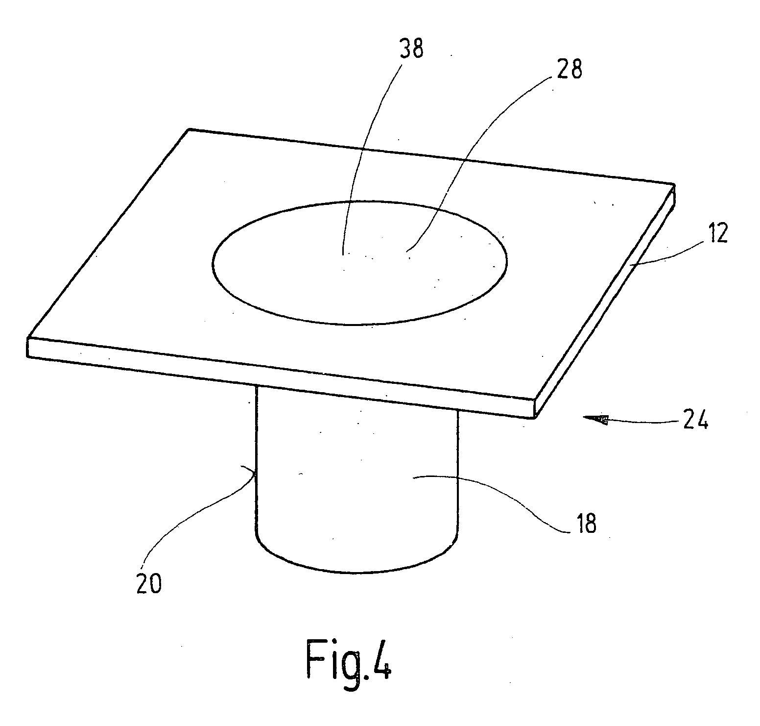
[0030] The silicon dioxide layer 14 serves as an etching stop in trench etching of the micromechanical structures into the structured layer 16. The trench etching process uncovers a membrane, comprising...


PUM


Abstract

The invention relates to an integrated semiconductor component for high-frequency measurements and to the use thereof.
It is provided that the semiconductor component is a component of a semiconductor circuit (10) comprising a first silicon layer (12), an adjoining silicon dioxide layer (insulating layer (14)) and a subsequent further silicon layer (structured layer (16)) (SOI wafer), and the semiconductor component comprises an IMPATT oscillator (30), having a resonator (24) which includes a metallized cylinder (18) of silicon, disposed in the structured layer (16); a coupling disk (28) covering the cylinder (18) in the region of the first layer (12); and an IMPATT diode (32), communicating with the cylinder (18) of the resonator (24) via a recess (38) in the coupling disk (28); and a reference oscillator (46) of lower frequency, having a resonator (24) which includes a metal cylinder (18) of silicon, disposed in the structured layer (16), and coupling disk (28) covering the cylinder in the region of the first layer (12); and a microwave conductor, communicating with the cylinder (18) of the resonator (24) via a recess (38) in the coupling disk (28), and the reference oscillator, via an active oscillator circuit (58), serves the purpose of frequency stabilization of the IMPATT oscillator (30); with integrated Schottky diodes; and a transmitting and receiving antenna (49).

Description

[0001] The invention relates to an integrated semiconductor component for high-frequency measurements and to the use thereof. PRIOR ART [0002] Semiconductor technology is increasingly being used in the automotive field. Miniaturization not only makes improved control and regulating technology for motor-specific functions possible but also opens up the path to new safety and riding comfort systems, such as parking aids, precrash and side crash functions, blind spot detection, fill level measurements, and distance measurements. For all the control—and regulation-related events, a sensor system—miniaturized as much as possible—must be available in the motor vehicle. [0003] As a rule, for the above fields of application named as examples, contactless sensors are used, which output a measurement beam of a defined frequency which is reflected from the object to be measured and is detected again by means of a receiver unit and evaluated. [0004] For fill level measurements, measuring instru...

Claims


Application Information

Patent Timeline
IPC IPC(8): H01L21/822G01S7/03G01S13/08H01L23/66H01L27/04H01L29/864H01P7/04H01Q9/04H01Q19/06H01Q23/00H03B9/14
CPCG01S7/032H01L23/66H01L29/864H01L2224/16145H01Q9/0435H01Q19/062H01Q23/00H01L2924/12032H03B9/14H03B9/147H01L2924/01068H01L2924/00H03B5/12
Inventor SCHMIDT, EWALDPFIZENMAIER, HEINZIRION, HANSHASCH, JUERGEN
Owner ROBERT BOSCH GMBH
Why Eureka
Try Eureka