Solid state image sensing device

a sensing device and solid state technology, applied in the direction of radio frequency control devices, instruments, television systems, etc., can solve the problems of incorrect color reproduction distortion of the picked-up image, and malfunction of the camera-equipped mobile phon

Active Publication Date: 2005-01-06
RENESAS ELECTRONICS CORP
View PDF7 Cites 45 Cited by
  • Summary
  • Abstract
  • Description
  • Claims
  • Application Information

AI Technical Summary

Benefits of technology

[0016] The present invention is made in order to solve the above-mentioned problems, and it is therefore an object of the present invention to provide a solid state image sensing device which offers strengthened resistance to EMC noises and provides improved stability of operation with a simple structure.
[0018] Therefore, the solid state image sensing device according to the present invention can supply a stable power supply voltage and a stable power supply current to each of the solid state image sensor and the integrated circuit chip, and can make the image pickup function thereof work with stability.

Problems solved by technology

Electric waves emitted out of such a camera-equipped mobile phone may cause electromagnetic induction in each of the circuits mounted in the mobile phone, and this electromagnetic induction may cause the camera-equipped mobile phone to malfunction.
As a result of the malfunction, there cause signs of trouble, such as a striped pattern which appears in a picked-up image, distortion of the picked-up image, improper color reproduction of the picked-up image, and reduction in the signal-to-noise ratio of the picked-up image.
In addition, there is a possibility that a passing through current noise peculiar to CMOS circuits, which has occurred in a digital circuit of the camera-equipped mobile phone flows into an image pickup processing circuit by way of power supply electric lines, and can reduce the signal-to-noise ratio of the picked-up image.
Unnecessary radiation of electromagnetic waves may occur from the solid state image sensing device mounted in the mobile phone, and may induce other circuits mounted in the mobile phone and produce noises.
As a result, such unnecessary radiation of electromagnetic waves from the solid state image sensing device may cause the other circuits mounted in the mobile phone to malfunction.
As can be seen from the above description, a problem with a prior art solid state image sensing device constructed as above is that while EMC measures are not adequately taken in design stages and EMC measures are hardly installed in design stages for either a module or package in which a solid state image sensor is mounted, the widening of the power supply electric lines, which is carried out as EMC measures, causes an increase in the size of the solid state image sensor and the size of a printed wiring board on which the solid state image sensor is mounted, the enclosing of the solid state image sensor and other components with a shielding member, such as a metal plate, causes an increase in the sizes of those components, as well as an increase in the weights of the components.
Another problem is that since additional material costs and additional manufacturing processes are needed for the EMC measures, the manufacturing cost is increased.

Method used


Image

  • Solid state image sensing device
  • Solid state image sensing device
  • Solid state image sensing device

Examples


embodiment 1

[0034]

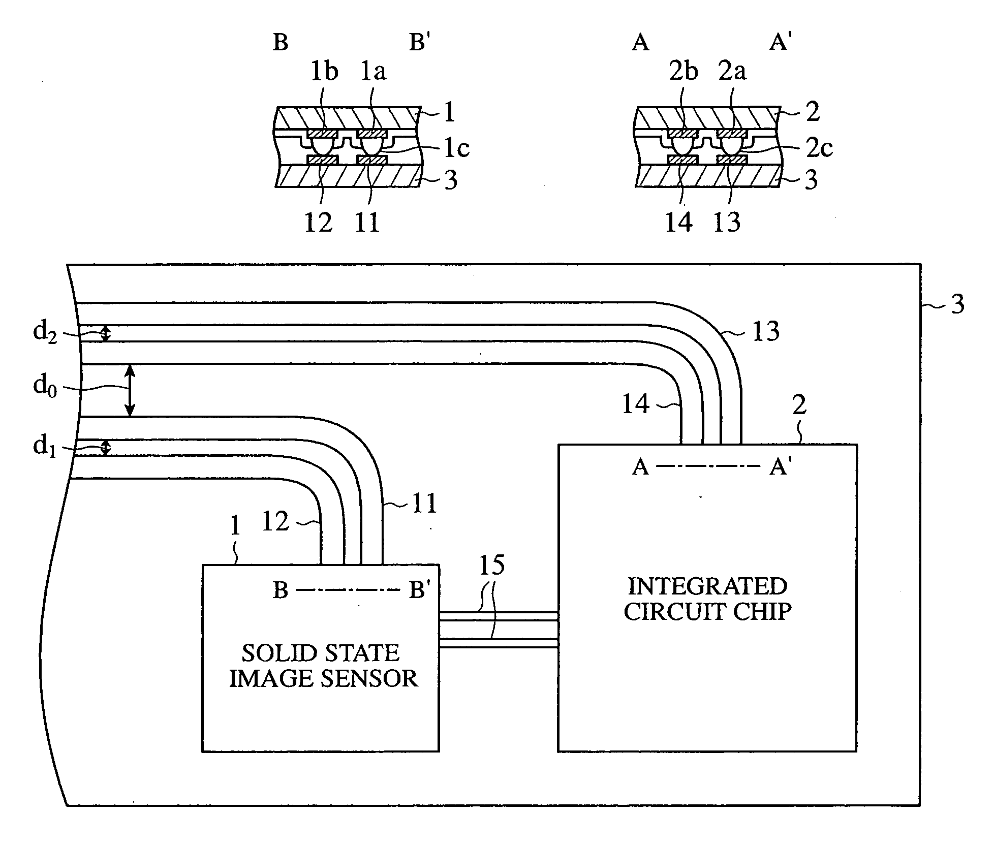
[0035]FIG. 1 is an explanatory drawing showing the structure of a solid state image sensing device according to embodiment 1 of the present invention. A part of a flexible wiring board on which a solid state image sensor and an integrated circuit chip are mounted is illustrated in FIG. 1, and an illustration of signal electric lines other than power supply electric lines, except for a part of the signal electric lines, is omitted.

[0036] The solid state image sensor 1 and the integrated circuit chip 2 as shown in FIG. 1 are flip-chip bonded on a side surface of the flexible wiring board 3 on which printed wiring is formed. High-potential and low-potential power supply electric lines are formed on the side surface of the flexible wiring board 3. Each high-potential power supply electric line can supply a power supply potential of 2.8V to either the solid state image sensor 1 or the integrated circuit chip 2, and each low-potential power supply electric line can supply a ground ...

embodiment 2

[0048]

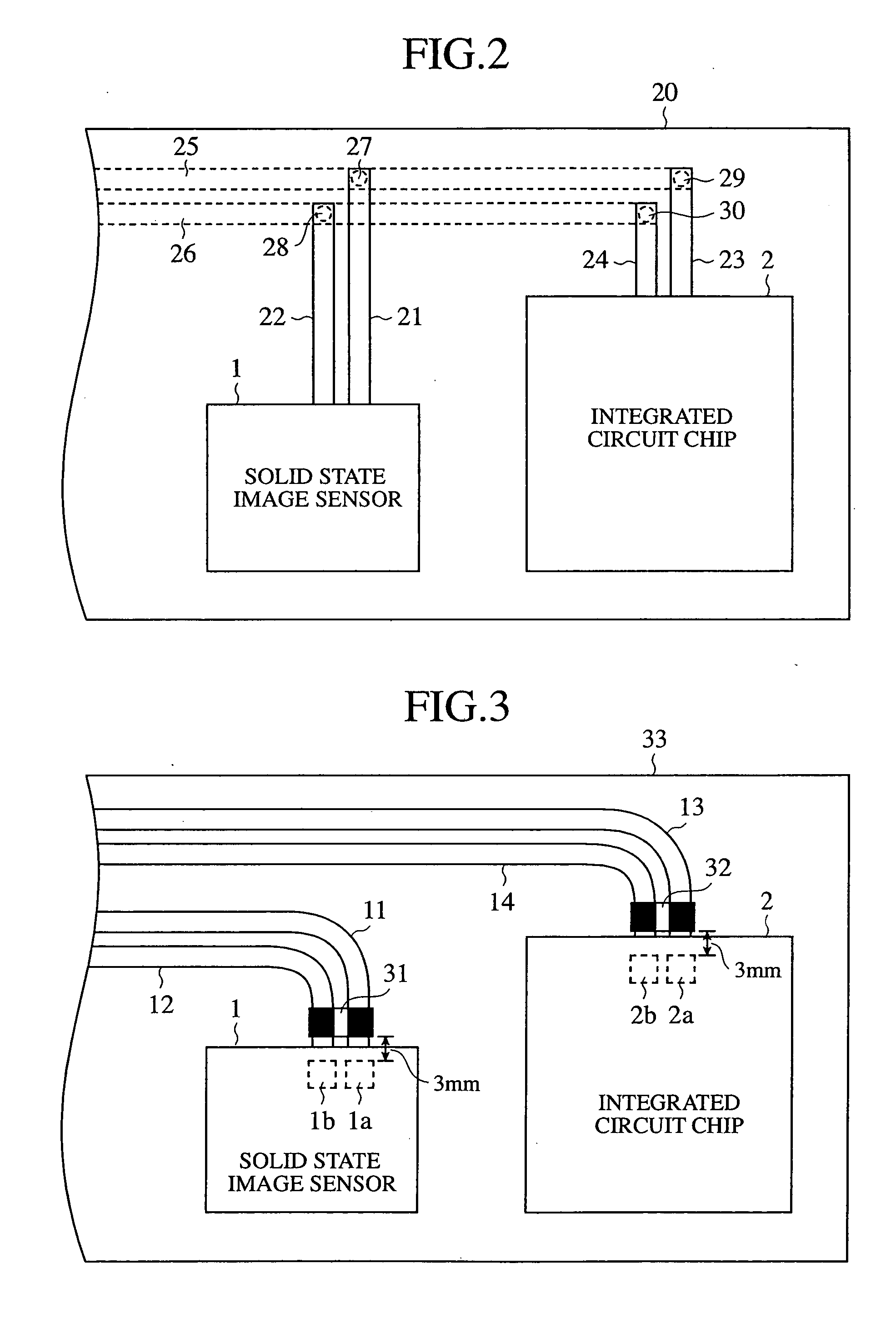
[0049]FIG. 2 is an explanatory drawing showing the structure of a solid state image sensing device in accordance with embodiment 2 of the present invention. The same components as those of the solid state image sensing device of embodiment 1 as shown in FIG. 1, and like components are designated by the same reference numerals as shown in FIG. 1, and therefore the explanation of those components will be omitted hereafter. In FIG. 1, a part of a wiring board on which one solid state image sensor and one integrated circuit chip are mounted is illustrated, and an illustration of signal lines other than power supply electric lines is omitted.

[0050] The solid state image sensor 1 and the integrated circuit chip 2 as shown in FIG. 2 are flip-chip mounted on the flexible wiring board 20 having front and back surfaces on each of which printed wiring is formed. Each of the solid state image sensor 1 and the integrated circuit chip 2 has a power supply pad for connecting with a high-pot...

embodiment 3

[0058]

[0059]FIG. 3 is an explanatory drawing showing the structure of a solid state image sensing device according to embodiment 3 of the present invention. In the figure, the same components as those of the solid state image sensing device of embodiment 1 as shown in FIG. 1, and like components are designated by the same reference numerals as shown in FIG. 1, and therefore the explanation of those components will be omitted hereafter. In FIG. 3, a part of a wiring board on which one solid state image sensor and one integrated circuit chip are mounted is illustrated, and an illustration of signal lines other than power supply electric lines is omitted.

[0060] In accordance with this embodiment 3, the flexible wiring board 33 having a side surface on which printed wiring is formed, as shown in FIG. 3, corresponds to the flexible wiring board 3 shown in FIG. 1 on which capacitors 31 and 32 are disposed. In other words, the flexible wiring board 33 has the same structure as that explai...


PUM


Abstract

Each of a pair of power supply electric lines (11 and 12) connected to power supply pads of a solid state image sensor (1) and a pair of power supply electric lines (13 and 14) connected to power supply pads of an integrated circuit chip (2) is arranged so that the power supply electric lines included in each power supply electric line pair are in parallel with each other and has a very small gap between them. The power supply electric lines (11 to 14) have a certain width and bend portions that are curved smoothly with a predetermined curvature or less and are formed on a flexible wiring board (3). In each of the solid state image sensor (1) and the integrated circuit chip (2), the high-potential and low-potential power supply pads are arranged side by side.

Description

BACKGROUND OF THE INVENTION [0001] 1. Field of the Invention [0002] The present invention relates to a solid state image sensing device in which Electromagnetic compatibility (referred to as EMC from here on) measures, i.e., Electromagnetic interference (referred to as EMI from here on) and Electromagnetic susceptibility (referred to as EMS from here on) measures are taken. [0003] 2. Description of Related Art [0004] Most of solid state image sensing devices are constructed as a so-called multi-chip module in which a solid state image sensor and two or more integrated circuit chips are disposed on a printed wiring board, and are used for camcorder recording apparatus, digital cameras, camera-equipped personal digital assistants, camera-equipped mobile phones, and so on. Therefore, a downsizing of solid state image sensing devices has been required. [0005] For example, a camera-equipped mobile phone has a housing having a very small mounting area and a very small mounting volume, in ...

Claims


Application Information

Patent Timeline
Patent Type & Authority Applications(United States)
IPC IPC(8): H01L23/00H01L27/146H04N5/225H04N5/335H04N5/357H04N5/376H05K1/02
CPCH04N5/23241H04N5/2251H04N25/709H01L27/146H01L23/00
Inventor SHINOMIYA, KOHJI
Owner RENESAS ELECTRONICS CORP
Why Eureka
Try Eureka