Composition of plasma display panel

a technology of plasma display panel and display panel, which is applied in the field of plasma display panel composition, can solve the problems of jitter occurrence of pdp display device, interference with high speed driving, and limitation of increasing the electric permittivity of pbo-based dielectric material, and achieve the effect of reducing jitter

Inactive Publication Date: 2005-01-06
LG ELECTRONICS INC
View PDF5 Cites 6 Cited by
  • Summary
  • Abstract
  • Description
  • Claims
  • Application Information

AI Technical Summary

Benefits of technology

[0037] Therefore, one object of the present invention is to provide a composition of a plasma display panel (PDP) capable of effectively reducing a jitter.
[0038] Another object of the present invention is to provide a composition of a PDP capable of preventing jitter occurrence and mis-discharging by increasing an electric permittivity of a dielectric to its maximum and increasing a capacitance.
[0039] Still another object of the present invention is to provide a composition of a PDP capable of heightening a luminance and an efficiency by reflecting a portion of a visible ray radiated from a fluorescent material.

Problems solved by technology

Commonly, the PDP display device has a problem of jitter occurrence.
The jitter phenomenon, which occurs as discharging is delayed for a certain time for a specific applied scan pulse, causes a mis-discharging and interferes a high speed driving.
However, since a withstand voltage is reduced according to the increase in the electric permittivity, there is a limitation in increasing the electric permittivity of the PbO-based dielectric material (the material of the upper dielectric layer and the lower dielectric layer).
In addition, in the case of increasing the capacitance by reducing the thickness of the material having the same electric permittivity, a problem arises that the conventional dielectric can not withstand the withstand voltage of about 560V.
Thus, the electric permittivity of the dielectric can not be increased to its maximum.
In addition, if the thickness of the upper dielectric layer and the lower dielectric layer is reduced, the withstand voltage would be lowered down, causing the problem that jitter can not be effectively reduced, and thus, a high speed driving is hardly performed.

Method used


Image

  • Composition of plasma display panel
  • Composition of plasma display panel
  • Composition of plasma display panel

Examples


first embodiment

[0060] First Embodiment

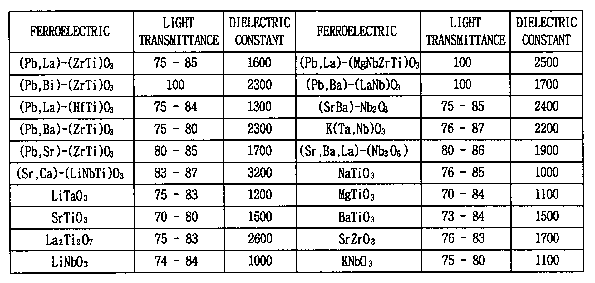
[0061] In the first embodiment, at least one of ferroelectric transparent ceramics materials of FIG. 3 is applied to the lower dielectric of the PDP. And the ferroelectric transparent ceramics powder is mixed in the conventional lower dielectric material or a ferroelectric transparent ceramics thin film is additionally formed on the conventional lower dielectric layer to increase a capacitance.

[0062] First, ferroelectric transparent ceramics powder is prepared and mixed to the lower dielectric material.

[0063] When the ferroelectric transparent ceramics powder is mixed in the lower dielectric material, the ferroelectric transparent ceramics powder with a particle diameter of a few μm is mixed in a range of 1 weight %˜20 weight % in parent glass powder. The ratio of the lower dielectric composition has been obtained by assuming the weight of the lower dielectric layer is 100 wt %.

[0064] Thereafter, the mixed powder is formed to a paste with a viscosity of abo...

second embodiment

[0068] Second Embodiment

[0069] In a second embodiment of the present invention, at least one of ferroelectric transparent ceramics materials shown in FIG. 3 is applied to the upper dielectric of the PDP. In addition, the ferroelectric transparent ceramics powder is mixed in the conventional upper dielectric material or a ferroelectric transparent ceramics thin film is additionally formed on the conventional upper dielectric layer in order to increase a capacitance.

[0070] First, ferroelectric transparent ceramics powder is prepared and mixed to the upper dielectric material.

[0071] When the ferroelectric transparent ceramics powder is mixed in the lower dielectric material, the ferroelectric transparent ceramics powder with a particle diameter of a few nm is mixed in a range of 1 wt %˜5 wt % in parent glass powder. The ratio of the upper dielectric composition has been obtained by assuming the weight of the upper dielectric layer is 100 wt %.

[0072] Thereafter, the mixed powder is f...

third embodiment

[0075] Third Embodiment

[0076] In the third embodiment of the present invention, at least one of ferroelectric transparent ceramics material shown in FIG. 3 is applied to a fluorescent material of the PDP. The ferroelectric transparent ceramics material is mixed in power form to a conventional fluorescent material or a ferroelectric transparent ceramics thin film is additionally formed on the conventional fluorescent material, to thereby increasing a capacitance.

[0077] First, ferroelectric transparent ceramics powder is prepared and mixed to the fluorescent material.

[0078] When the ferroelectric transparent ceramics powder is mixed to the fluorescent material, the fine ferroelectric transparent ceramics powder with a particle diameter of a few nm is mixed in a range of 1 wt %˜10 wt % in the fluorescent material powder. The ratio of the fluorescent material composition has been obtained by assuming the weight of the fluorescent layer is 100 wt %.

[0079] When the ferroelectric transp...


PUM

PropertyMeasurementUnit
visible ray transmittanceaaaaaaaaaa
reflectanceaaaaaaaaaa
particle diameteraaaaaaaaaa

Abstract

A composition of a plasma display panel (PDP) is disclosed. In order to effectively reduce a jitter, the composition contains a ferroelectric transparent ceramics material.

Description

BACKGROUND OF THE INVENTION [0001] 1. Field of the Invention [0002] The present invention relates to a plasma display panel (PDP) and, more particularly, to a composition of plasma display panel. [0003] 2. Description of the Background Art [0004] In general, a plasma display panel (PDP) device receives much attention as a next-generation display device together with a thin film transistor (TFT), a liquid crystal display (LCD), an EL (Electro-Luminescence) device, an FED (Field Emission Display) and the like. [0005] The PDP is a display device which uses a luminescent phenomenon according to an energy difference made when red, green and blue fluorescent materials are changed from an excited state to a ground state after being excited by 147 nm of ultraviolet rays which are generated as a He+X3 gas or N3+X3 gas is discharged from a discharge cell isolated by a barrier rib. [0006] Thanks to its properties of facilitation in manufacturing from a simple structure, a high luminance, a hig...

Claims


Application Information

Patent Timeline
Patent Type & Authority Applications(United States)
IPC IPC(8): C04B35/00B32B9/04C04B35/495H01J11/22H01J11/34H01J11/38H01J11/42
CPCH01J11/12H01J11/38Y10T428/265H01J11/42
Inventor LEE, YOON
Owner LG ELECTRONICS INC
Why Eureka
Try Eureka