

Method of resetting AP pinned layers with a canted field
- Summary
- Abstract
- Description
- Claims
- Application Information
AI Technical Summary
Benefits of technology
Problems solved by technology
Method used
Image

Examples
Embodiment Construction
Magnetic Disk Drive
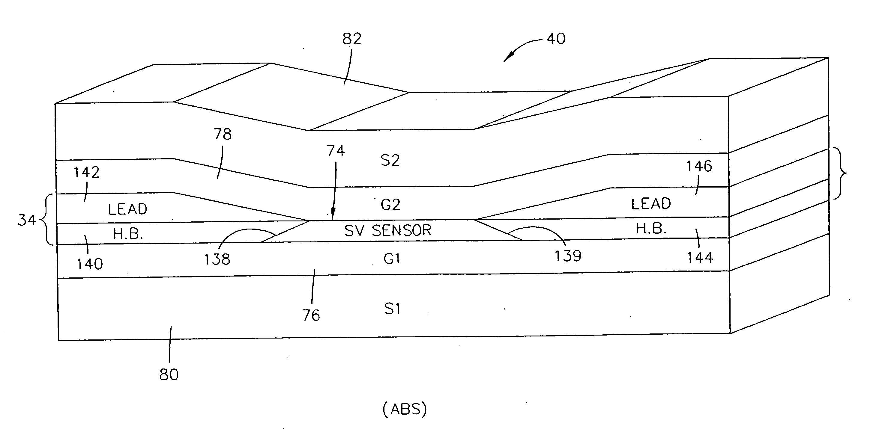
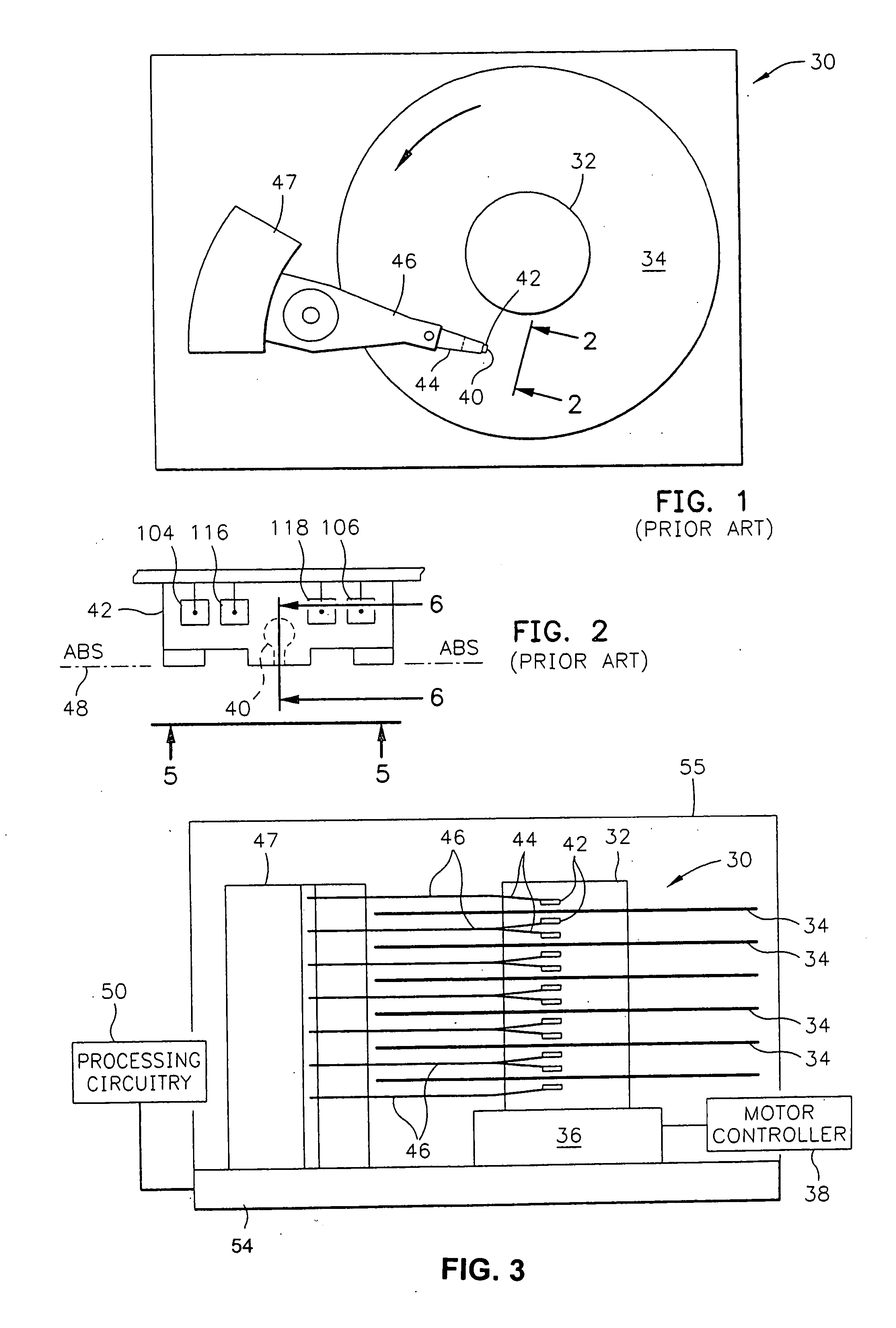
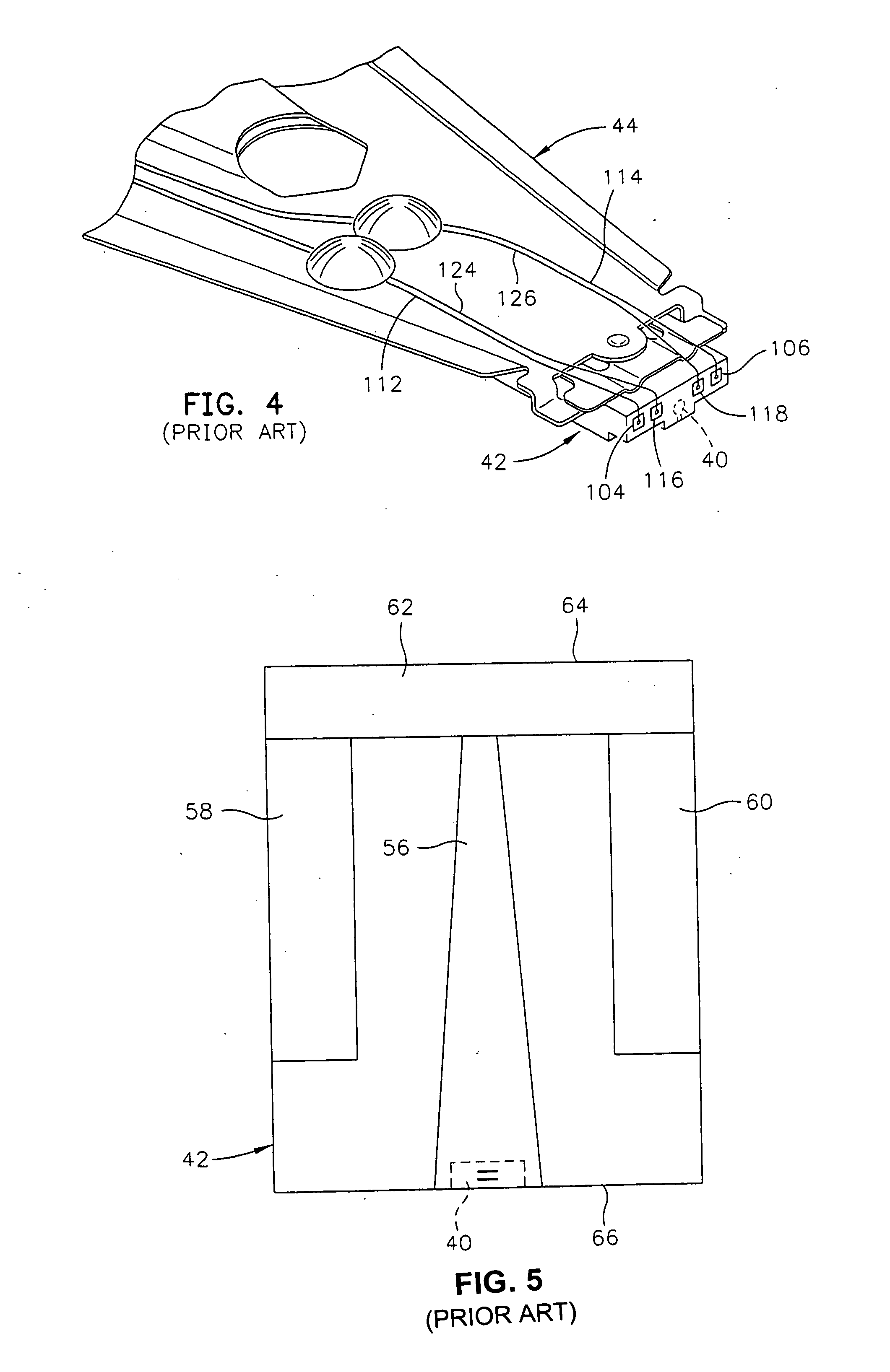
[0045] Referring now to the drawings wherein like reference numerals designate like or similar parts throughout the several views, FIGS. 1-3 illustrate a magnetic disk drive 30. The drive 30 includes a spindle 32 that supports and rotates a magnetic disk 34. The spindle 32 is rotated by a spindle motor 36 that is controlled by a motor controller 38. A slider 42 has a combined read and write magnetic head 40 and is supported by a suspension 44 and actuator arm 46 that is rotatably positioned by an actuator 47. A plurality of disks, sliders and suspensions may be employed in a large capacity direct access storage device (DASD) as shown in FIG. 3. The suspension 44 and actuator arm 46 are moved by the actuator 47 to position the slider 42 so that the magnetic head 40 is in a transducing relationship with a surface of the magnetic disk 34. When the disk 34 is rotated by the spindle motor 36 the slider is supported on a thin (typically, 0.01 μm) cushion of air (air be...
PUM
| Property | Measurement | Unit |
|---|---|---|
| Angle | aaaaa | aaaaa |
| Angle | aaaaa | aaaaa |
| Angle | aaaaa | aaaaa |
Abstract
Description
Claims
Application Information