Flange for integrated circuit package

Active Publication Date: 2005-01-20
IONIC MATERIALS INC
View PDF18 Cites 6 Cited by
  • Summary
  • Abstract
  • Description
  • Claims
  • Application Information

AI Technical Summary

Benefits of technology

[0018] Compositions of the flange, frame and leads provide matching coefficients of thermal expansion (CTE), thus reducing stress on the respective junctions between these parts. These compositions also provide good thermal conductivity by the flange and good electrical conductivity by the leads and the flange. In one embodiment, the flange is made with a high copper content, augmented by a small amount of zirconium, silver or other material. In another

Problems solved by technology

The high temperature used to attach a die to a flange can damage or deform plastic, however ceramic materials are able to withstand this high temperature.
This process is very expensive, and the thermal conductivity of the resulting alloy is limited.
Improved thermal conductivity can be achieved through the use of copper-molybdenum-copper laminated flanges fabricated by an

Method used


Image

  • Flange for integrated circuit package
  • Flange for integrated circuit package
  • Flange for integrated circuit package

Examples


Example

[0038] The contents of application Ser. No. 10 / 767,309, filed Jan. 29, 2004, and the contents of provisional Application No. 60 / 443,470, filed Jan. 29, 2003, are hereby incorporated by reference.

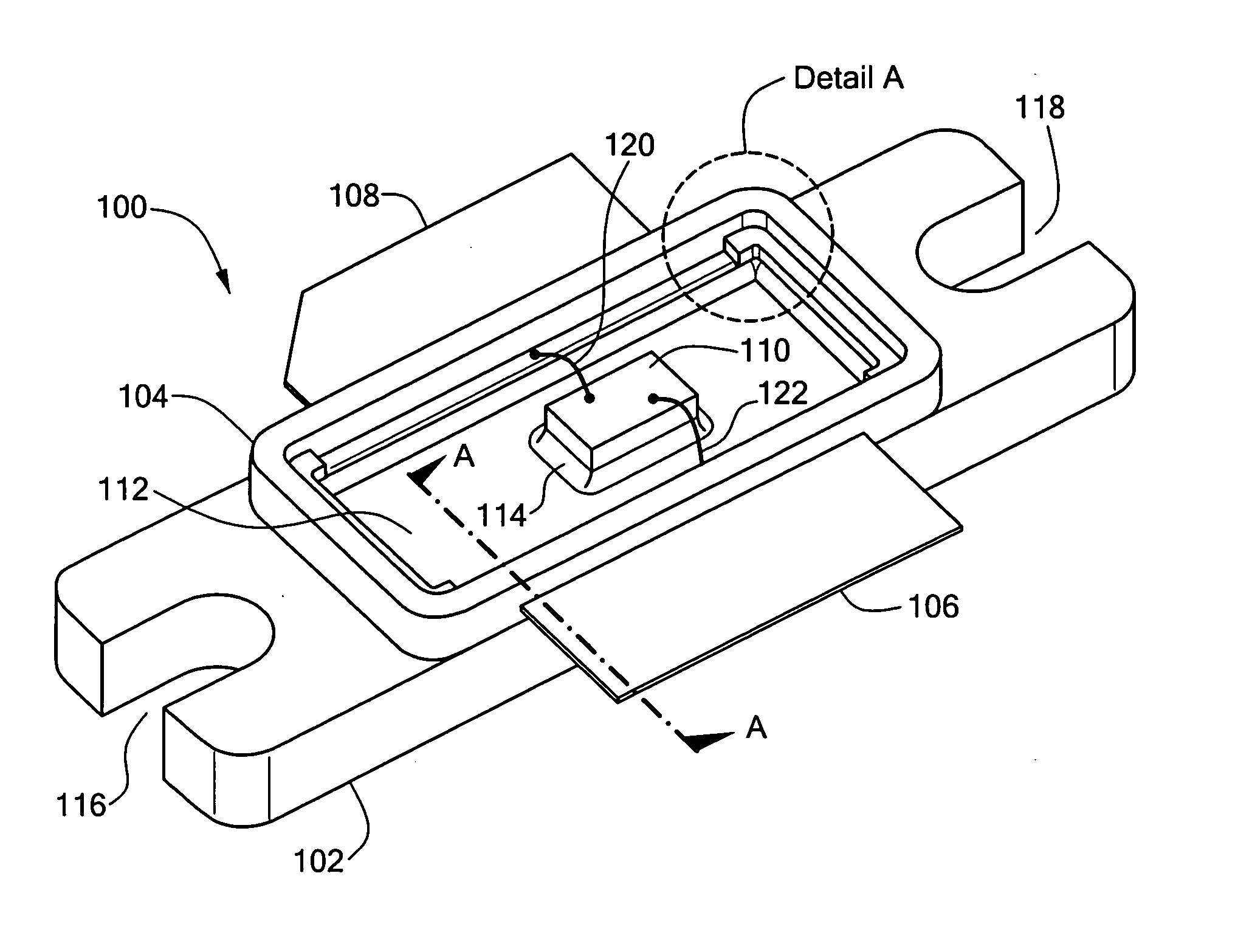
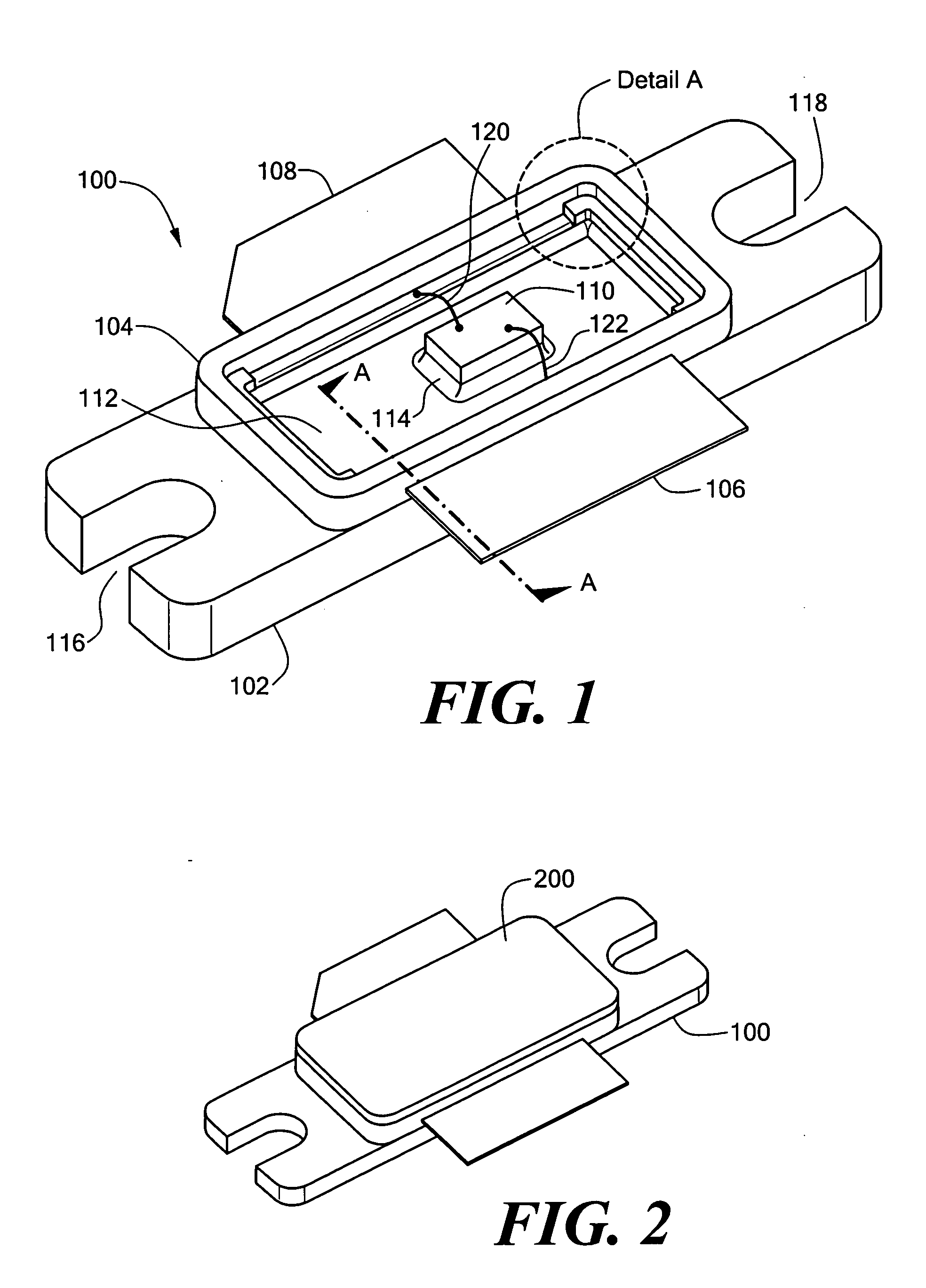
[0039] The present invention provides a low piece-count circuit package that can withstand high die-attach temperatures and can provide a hermetically sealed air cavity for a die, without the use of adhesives. FIG. 1 shows an exemplary circuit package 100, according to one embodiment of the present invention. For clarity, the circuit package 100 is shown without a lid. The circuit package 100 includes a flange 102, a frame 104 and two leads 106 and 108. The frame 104 electrically insulates the leads 106 and 108 from the flange 102 and each other. A die 110 is attached to a die-attach area 112, such as by eutectic solder 114. For clarity, FIG. 1 shows only one die, although typically two or more die can be attached to the die-attach area 112.

[0040] The eutectic solder 114 electrically bonds...


PUM


Abstract

A circuit package for housing semiconductor or other integrated circuit devices (“die”) includes a high-copper flange, one or more high-copper leads and a liquid crystal polymer frame molded to the flange and the leads. The flange includes a dovetail-shaped groove or other frame retention feature that mechanically interlocks with the molded frame. During molding, a portion of the frame forms a key that freezes in or around the frame retention feature.

Description

CROSS REFERENCE TO RELATED APPLICATIONS [0001] This application is a divisional of application Ser. No. 10 / 767,309, filed Jan. 29, 2004, which claims the benefit of provisional Application No. 60 / 443,470, filed Jan. 29, 2003.STATEMENT REGARDING FEDERALLY SPONSORED RESEARCH OR DEVELOPMENT [0002] Not Applicable BACKGROUND OF THE INVENTION [0003] This application relates to circuit packages for integrated circuits and, more particularly, to circuit packages that include metal flanges and high-temperature thermoplastic frames. [0004] Semiconductor and other integrated circuit devices (sometimes referred to as “chips” or “die”) are typically mounted inside circuit packages to protect the die and to facilitate electrically, mechanically and thermally connecting the die to printed circuit boards, heat sinks and the like. A typical circuit package includes a base (commonly referred to as a “slug” or “flange”), a protective insulating housing and leads extending through the housing. Inside t...

Claims


Application Information

Patent Timeline
IPC IPC(8): H01L23/047H01L23/10H01L23/492H01L23/498
CPCH01L21/50Y10T428/24132H01L23/10H01L23/492H01L23/49861H01L23/562H01L23/564H01L24/29H01L24/48H01L24/85H01L2224/32506H01L2224/48247H01L2224/85205H01L2924/01012H01L2924/0102H01L2924/01078H01L2924/01079H01L2924/14H01L2924/16195H01L2924/16315H01L2924/18301H01L2924/3511H01L2924/01322H01L2924/10253H01L23/047H01L2224/73265H01L2924/3512H01L2924/00H01L2924/12042H01L2224/45099H01L2924/00014H01L2924/181H01L21/4842H01L21/4817H01L23/49541H01L2224/45015H01L2924/207H01L23/28H01L23/043
Inventor ZIMMERMAN, MICHAEL
Owner IONIC MATERIALS INC
Why Eureka
Try Eureka