[0020] Reference will now be made in detail to the present preferred embodiments of the invention, examples of which are illustrated in the accompanying drawings. Wherever possible, the same reference numbers are used in the drawings and the description to refer to the same or like parts.
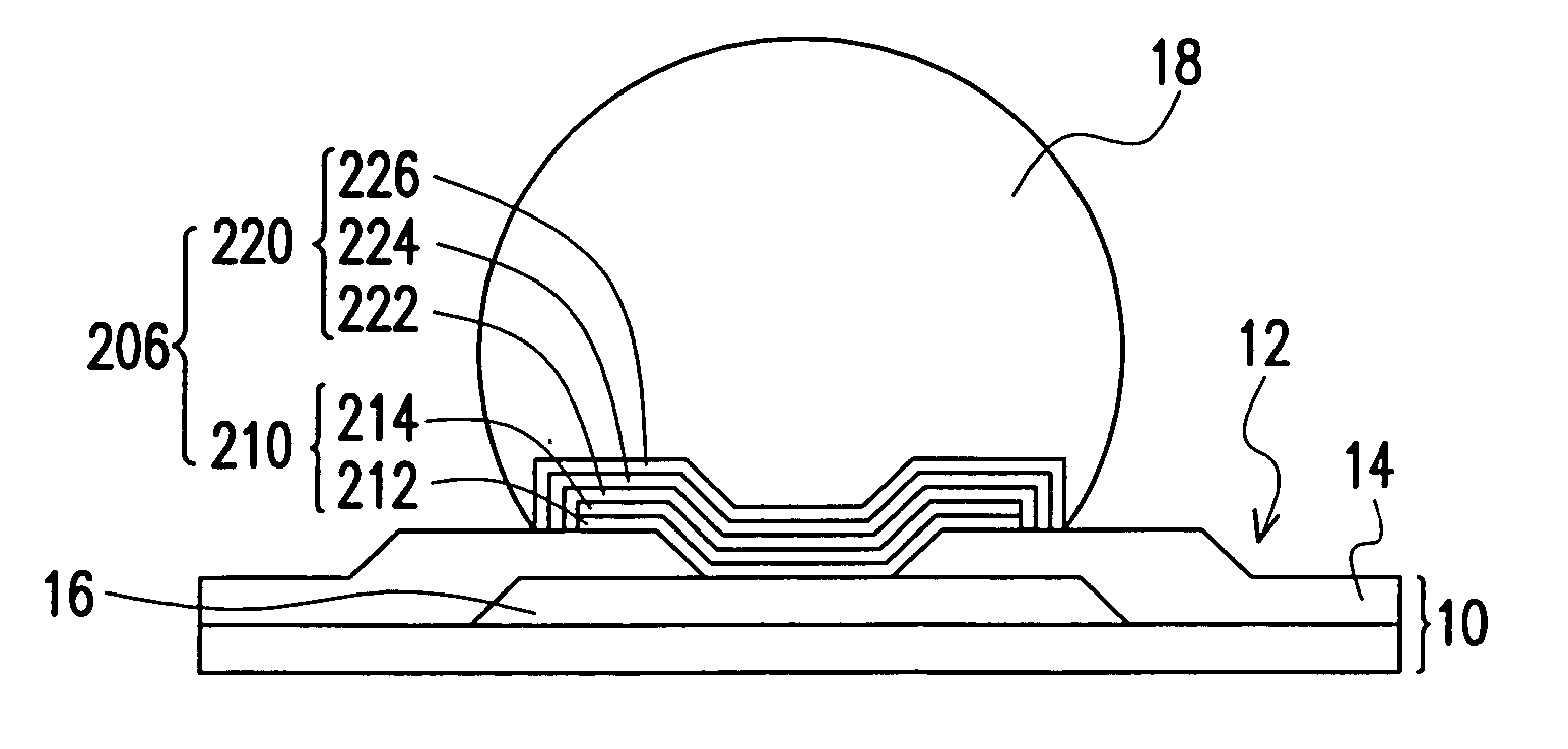
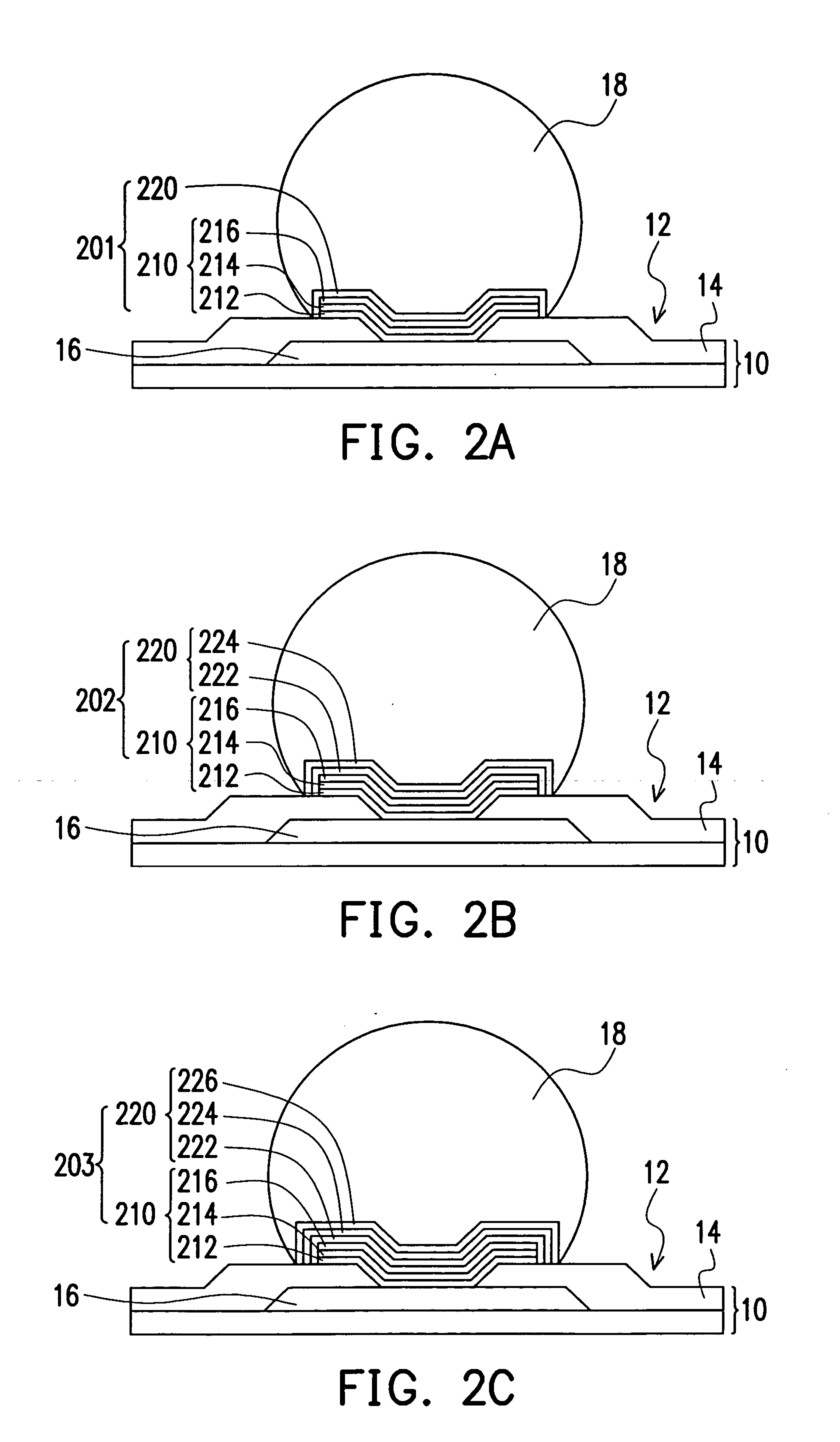
[0021]FIG. 2A is a schematic cross-sectional view showing a first type of under-bump metallurgical structure between the bonding pad of a die and a solder bump according to a preferred embodiment of this invention. As shown in FIG. 2A, the die 10 has an active surface 12 with a passivation layer 14 and a plurality of bonding pads 16 (only one is shown) thereon. The passivation layer and the bonding pads 16 are formed over the active surface 12 of the die 10 such that the passivation layer 14 exposes the bonding pads 16. Note that the active surface 12 of the die 10 refers to the side where all active devices are formed. To provide an interface for joining the bonding pad 16 and the solder bump 18 together, this invention proposes a first type of under-bump metallurgical structure 201 between the bonding pad 16 and the solder bump 18. The first type of under-bump metallurgical structure 201 includes a metallic layer 210 and a buffer metallic layer (or an inter-metallic compound growth buffer layer) 220. The metallic layer 210 is formed over the bonding pad 16 and the buffer metallic layer 220 is formed between the metallic layer 210 and the solder bump 18. In addition, the metallic layer 210 further includes an adhesion layer 212, a barrier layer 214 and a wettable layer 216. The adhesion layer 212 is formed over the bonding pad 16, the barrier layer 214 is formed over the adhesion layer 212 and the wettable layer 216 is formed between the barrier layer 214 and the buffer metallic layer 220. Since the metallic layer 210 has a material and structural composition identical to the under-bump metallic layer 100 as shown in FIG. 1, detailed description is not repeated here.
[0022] In general, the wettable layer 216 is made from a material including copper or gold. If the wettable layer 216 is made from copper, an anti-oxidation layer (not shown) may be coated over the wettable layer 216 to prevent surface oxidation of the copper wettable layer 216. The anti-oxidation layer is commonly a thin layer of gold. However, if major constituents of the wettable layer 216 are copper, nickel or gold, the tin within the solder bump 18 may easily react chemically with copper, nickel or gold within the under-bump metallic layer 210 after a thermal treatment of the solder bump 18. Ultimately, a layer of inter-metallic compound is formed between the solder bump 18 and the under-bump metallic layer 210. In this invention, the buffer metallic layer 220 of the first type of under-bump metallurgical structure 210 is formed between the wettable layer 216 and the solder bump 18 so that growth of the inter-metallic compound is reduced.
[0023] To prevent the buffer metallic layer 220 from melting during thermal treatment (for example, a reflow operation) and losing its functional capacity, the buffer metallic layer 220 must have a melting point higher than the solder bump 18 so that buffer metallic layer 220 does not melt and is not completely dissolved into the solder bump 18 while the solder bump 18 is melting. Furthermore, to provide a good bonding strength between the buffer metallic layer 220 and the solder bump 18, the buffer metallic layer 220 must easily wet the solder bump 18. Thus, the buffer metallic layer 220 is preferably made from lead, a high melting point lead-tin alloy or some other materials.
[0024] In addition, the buffer metallic layer 220 may be principally constituent of one element of the composition of the solder bump 18. For an example, when the solder bump 18 is constituent of lead-tin alloy, the buffer metallic layer 220 may be principally constituent of lead or tin. For another example, when the solder bump 18 is constituent of lead-tin-copper alloy, the buffer metallic layer 220 may be principally constituent of lead, tin, or copper. In order to prevent the under-bump metallic layer 210 from being attacked by the solder bump 18, the thickness of the buffer metallic layer 220 is usually greater than that of under-bump metallic layer 210. For example, when the thickness of the under-bump metallic layer 210 is about 100 to 200 nm, the thickness of the buffer metallic layer 220 is greater than 1 micron, or about 0.5 micron to 5 microns. When the buffer metallic layer 220 may be principally constituent of one element of the composition of the solder bump 18, the alloy formed from the buffer metallic layer 220 with the solder bump 18 is similar to the composition of solder bump 18 with a continuous constitution gradient, so that no structure weak point forming when the top portion of the under-bump metallic layer 210 is not made of any one of the composition of the solder bumps 18.
[0025]FIGS. 2B and 2C are schematic cross-sectional views of the second and the third type of under-bump metallurgical structures between the bonding pad 16 of the die 10 and the solder bump 18. As shown in FIG. 2B, the second type of under-bump metallurgical structure 202 is very similar to the first type of under-bump metallurgical structure 201. The second type of under-bump metallurgical structure 202 similarly has the metallic layer 210 in the first type of under-bump metallurgical structure 201. However, the buffer metallic layer 220 further includes a first buffer metallic layer 222 and a second buffer metallic layer 224. The first buffer metallic layer 222, for example, is a lead layer formed over the wettable layer 216. The second buffer metallic layer 224, for example, is a tin layer formed between the first buffer metallic layer 222 and the solder bump 18. As shown in FIG. 2C, the third under-bump metallurgical structure 203 is also similar to the first type of under-bump metallurgical structure 201. The third under-bump metallurgical layer 203 similarly has the metallic layer 210 of the first under-bump metallurgical structure 201. However, the buffer metallic layer 220 further includes a first buffer metallic layer 222, a second buffer metallic layer 224 and a third buffer metallic layer 226. The first buffer metallic layer 222, for example, is a lead layer formed over the wettable layer 216. The second buffer metallic layer 224, for example, is a tin layer formed over the first buffer metallic layer 222. The third buffer metallic layer 226, for example, is a lead layer formed between the second buffer metallic layer 224 and the solder bump 18.
[0026]FIGS. 2D, 2E and 2F are cross-sectional views of the fourth, fifth and the sixth type of under-bump metallurgical structures between the bonding pad 16 of a die 10 and the solder bump 18. Since the buffer metallic layer 220 of the first type under-bump metallurgical structure 201 as shown in FIG. 2A is capable of wetting the solder bump 18, the wettable layer 216 may be omitted to form the fourth type of under-bump metallurgical structure as shown in FIG. 2D. Similarly, the buffer metallic layer 220 of the second under-bump metallurgical structure 202 as shown in FIG. 2B is capable of wetting the solder bump 18. Hence, the wettable layer 210 may be omitted to form the fifth under-bump metallurgical structure 205 as shown in FIG. 2E. Likewise, the buffer metallic layer 220 of the third under-bump metallurgical structure 203 is capable of wetting the solder bump 18. Consequently, the wettable layer 216 may be omitted to form the sixth type of under-bump metallurgical structure 206 as shown in FIG. 2F.
[0027]FIGS. 3A to 3G are schematic cross-sectional views showing the progression of steps for fabricating the first type of under-bump metallurgical structure as shown in FIG. 2A. As shown in FIG. 3A, the die 10 has an active surface 12 with a passivation layer 14 and a plurality of bonding pads 16 (only one is shown) thereon. The passivation layer and the bonding pads 16 are formed over the active surface 12 of the die 10 such that the passivation layer 14 exposes the bonding pads 16. As shown in FIG. 3B, a metallic film layer 302 is globally formed over the active surface 12 of the die 10, for example, by evaporation, sputtering or plating. The thin metallic layer 302 serves as a seed layer. As shown in FIG. 3C, a photoresist layer 304 is formed over the thin metallic layer 302 exposing a portion of the thin metallic layer 302 above the bonding pads 16. As shown in FIG. 3D, another metallic layer 306 is formed over the thin metallic layer 302 by plating, evaporation or sputtering, for example. The metallic layer 306 includes an adhesion layer, a barrier layer and a wettable layer. As shown in FIG. 3E, a buffer metallic layer 308 is formed over the metallic layer 306 by plating, for example. As shown in FIG. 3F, the patterned photoresist layer 304 is removed to expose the thin metallic layer 302 underneath but outside the metallic layer 306. Finally, as shown in FIG. 3G, a short etching operation is conducted to remove the thin metallic layer 302 outside the metallic layer 306, thereby forming the first type of under-bump metallurgical structure 201 as shown in FIG. 2A.
[0028] Note that the aforementioned paragraph only describes one of the processes that can be used to fabricate the first type of under-bump metallurgical structure 210. Since the steps for producing other types of under-bump metallurgical structures such as 202 to 206 as shown in FIGS. 2B to 2F are very similar, detail descriptions are omitted. In addition, this invention also permits the formation of a mini bump to replace the buffer metallic layer 220 of the under-bump metallurgical structure 201 in FIG. 2A for a further reduction of the growth of inter-metallic compound between the metallic layer and the solder bump.
[0029]FIG. 4A is a schematic cross-sectional view showing a seventh type of under-bump metallurgical structure between the bonding pad of a die and a solder bump according to a preferred embodiment of this invention. As shown in FIG. 4A, the seventh type of under-bump metallurgical structure 401 includes a metallic layer 410 and a mini bump 422. The metallic layer 410 is formed over a bonding pad 16 and the mini bump 422 is formed between the metallic layer 410 and the solder bump 18. The metallic layer 410 has a material composition identical to the metallic layer in the first type of under-bump metallurgical structure 201. Note that material compositions and properties of the mini bump 422 are identical to the buffer metallic layer 220 in FIG. 2A.
[0030]FIG. 4B is a schematic cross-sectional view showing an eighth type of under-bump metallurgical structure between the bonding pad of a die and a solder bump according to a preferred embodiment of this invention. As shown in FIG. 4B, the eighth type of under-bump metallurgical structure 402 has a smaller distribution area compared with the seventh type of under-bump metallurgical structure 401 in FIG. 4A. Hence, the solder bump 18 has a relatively smaller diameter and the pitch between neighboring solder bumps 18 can be reduced.
[0031]FIG. 4C is a schematic cross-sectional view showing a ninth type of under-bump metallurgical structure between the bonding pad of a die and a solder bump according to a preferred embodiment of this invention. As shown in FIG. 4C, the buffer metallic structure 420 of the ninth type of under-bump metallurgical structure 403 further includes a mini bump 422 and a buffer metallic layer 424. The mini bump 422 is formed over the metallic layer 410 and the buffer metallic layer 424 is formed between the mini bump 422 and the solder bump 18. The buffer metallic layer 424 is a tin layer, for example.
[0032]FIG. 4D is a schematic cross-sectional view showing a tenth type of under-bump metallurgical structure between the bonding pad of a die and a solder bump according to a preferred embodiment of this invention. As shown in FIG. 4D, the tenth type of under-bump metallurgical structure 404 has a smaller distribution area compared with the ninth type of under-bump metallurgical structure 403 in FIG. 4C. Hence, the solder bump 18 has a relatively smaller diameter and the pitch between neighboring solder bumps 18 can be reduced.
[0033]FIGS. 4E to 4H are schematic cross-sectional views showing an eleventh, a twelfth, a thirteenth and a fourteenth type of under-bump metallurgical structures between the bonding pad of a die and a solder bump according to a preferred embodiment of this invention. As shown in FIGS. 4E to 4H, the mini bump 422 of the eleventh to the fourteenth types of under-bump metallurgical structures 405 to 408 is capable of wetting the solder bump 18. Hence, the wettable layer 416 in the seventh to the tenth under-bump metallurgical structures as shown in FIGS. 4A to 4D can be omitted to form the eleventh to the fourteenth types of under-bump metallurgical structures. Since the mini bump 422 and the buffer metallic layer 424 has already been explained before, detail description is not repeated here.
[0034]FIGS. 5A to 5H are schematic cross-sectional views showing the progression of steps for fabricating the first type of under-bump metallurgical structure as shown in FIG. 4A. As shown in FIG. 5A, the die 10 has an active surface 12 with a passivation layer 14 and a plurality of bonding pads 16 (only one is shown) thereon. The passivation layer and the bonding pads 16 are formed over the active surface 12 of the die 10 such that the passivation layer 14 exposes the bonding pads 16. As shown in FIG. 5B, a metallic film layer 502 is globally formed over the active surface 12 of the die 10, for example, by evaporation, sputtering or plating. The thin metallic layer 502 serves as a seed layer. As shown in FIG. 5C, a photoresist layer 504 is formed over the thin metallic layer 502 exposing a portion of the thin metallic layer 502 above the bonding pads 16. As shown in FIG. 5D, another metallic layer 506 is formed over the thin metallic layer 502 by plating, evaporation or sputtering, for example. The metallic layer 506 includes an adhesion layer, a barrier layer and a wettable layer. As shown in FIG. 5E, a buffer metallic layer 508 is formed over the metallic layer 506 by plating or printing, for example. As shown in FIG. 5F, the patterned photoresist layer 504 is removed to expose the thin metallic layer 502 underneath but outside the metallic layer 506. As shown in FIG. 5G, a short etching operation is conducted to remove the thin metallic layer 502 outside the metallic layer 506. Finally, as shown in FIG. 5H, a reflow operation may be conducted to transform the buffer metallic layer 508 into a mini bump 508a that encloses the metallic layer 506. However, the aforementioned paragraph only describes one of the processes that can be used to fabricate the seventh type of under-bump metallurgical structure 401. Since the steps for producing other types of under-bump metallurgical structures such as 402 to 408 as shown in FIGS. 4B to 4H are very similar, detail descriptions are omitted.
[0035] The under-bump metallurgical structure according to this invention can be applied to a junction interface between the bonding pad of a die and a solder bump. The principle constituent of the solder bump is lead-tin alloy. The under-bump metallurgical structure includes a metallic layer and a buffer metallic structure. The metallic layer is formed over the bonding pads. The principle constituent of the metallic layer is copper, nickel or gold. The buffer metallic structure is formed between the metallic layer and the solder bump for reducing the growth of inter-metallic compound between the metallic layer and the solder bump. The buffer metallic structure may include a buffer metallic layer, a mini bump or a combination of the two. The buffer metallic structure is capable of wetting the solder bump and has a melting point higher than the solder bump. The buffer metallic structure is preferably made from lead.
[0036] About the material, the foregoing bump can also be made from a lead-free material, such as SnAg, SnAgBi, SnAgBiCu, SnAgBiCuGe, SnAgBiX, SnAgCu, SnBi, SnCu, SnZn, SnCuSbAg, SnSb or SnZnBi, and the under-bump metallurgical structure can include, for example, Sb, Ag, Sn/Ag, Sn/Cu, and so on. However, if the lead is incuded, it can include, for example, SnPbAg for the bump.
[0037] In conclusion, the under-bump metallurgical structure according to this invention is formed between a bonding pad and a solder bump. The under-bump metallurgical structure reduces chemical reaction between tin, a principle constituent within the solder bump, with other metallic materials within the under-bump metallic layer or metallic materials within the bonding pad to form inter-metallic compound. By reducing the growth of inter-metallic compound, electrical resistance between the under-bump metallurgical structure and the solder bump is reduced while bonding strength between the under-bump metallurgical structure and the solder bump is increased.
[0038] It will be apparent to those skilled in the art that various modifications and variations can be made to the structure of the present invention without departing from the scope or spirit of the invention. In view of the foregoing, it is intended that the present invention cover modifications and variations of this invention provided they fall within the scope of the following claims and their equivalents.