Wireless data communication demodulation device and demodulation method
- Summary
- Abstract
- Description
- Claims
- Application Information
AI Technical Summary
Benefits of technology
Problems solved by technology
Method used
Image

Examples
first embodiment
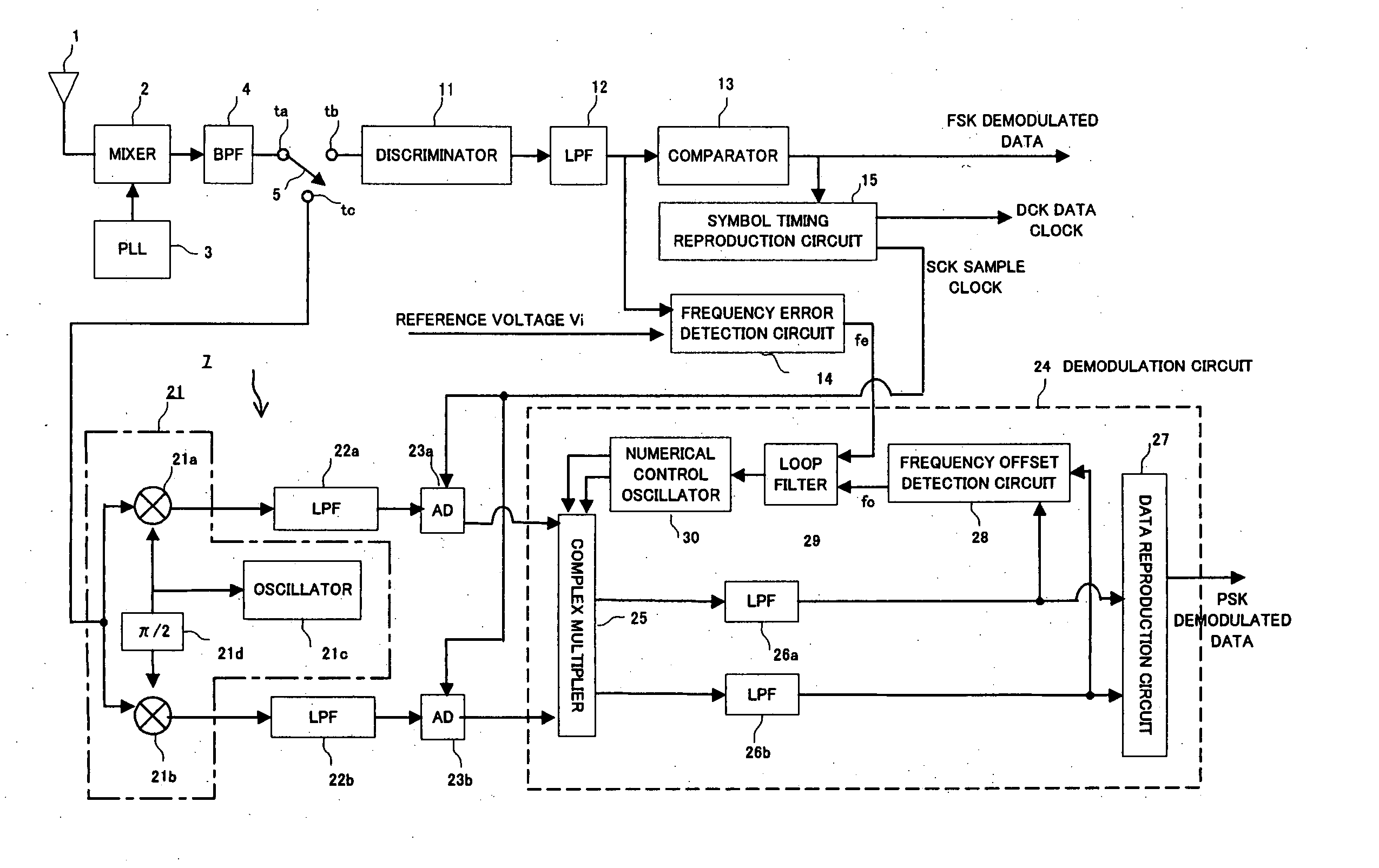
[0038]FIG. 1 is a block diagram showing the present invention and showing a wireless data communication demodulation device in the case in which the wireless data communication demodulation device is applied to a short distance wireless communication system which uses an ISM band of 2.4 GHz.
[0039] In the figure, reference sign WD denotes a wireless data communication demodulation device. This wireless data communication demodulation device WD includes a receiving antenna 1 and receives a transmission packet shown in FIG. 2, which is sent from a transmission side, with this receiving antenna 1. The received signal is supplied to a mixer 2 and is multiplied by a local oscillation signal, which is inputted from a phase locked loop (hereinafter referred to as PLL) circuit 3 and subjected to down-convert to be converted into an intermediate frequency signal (IF signal) by this mixer 2.
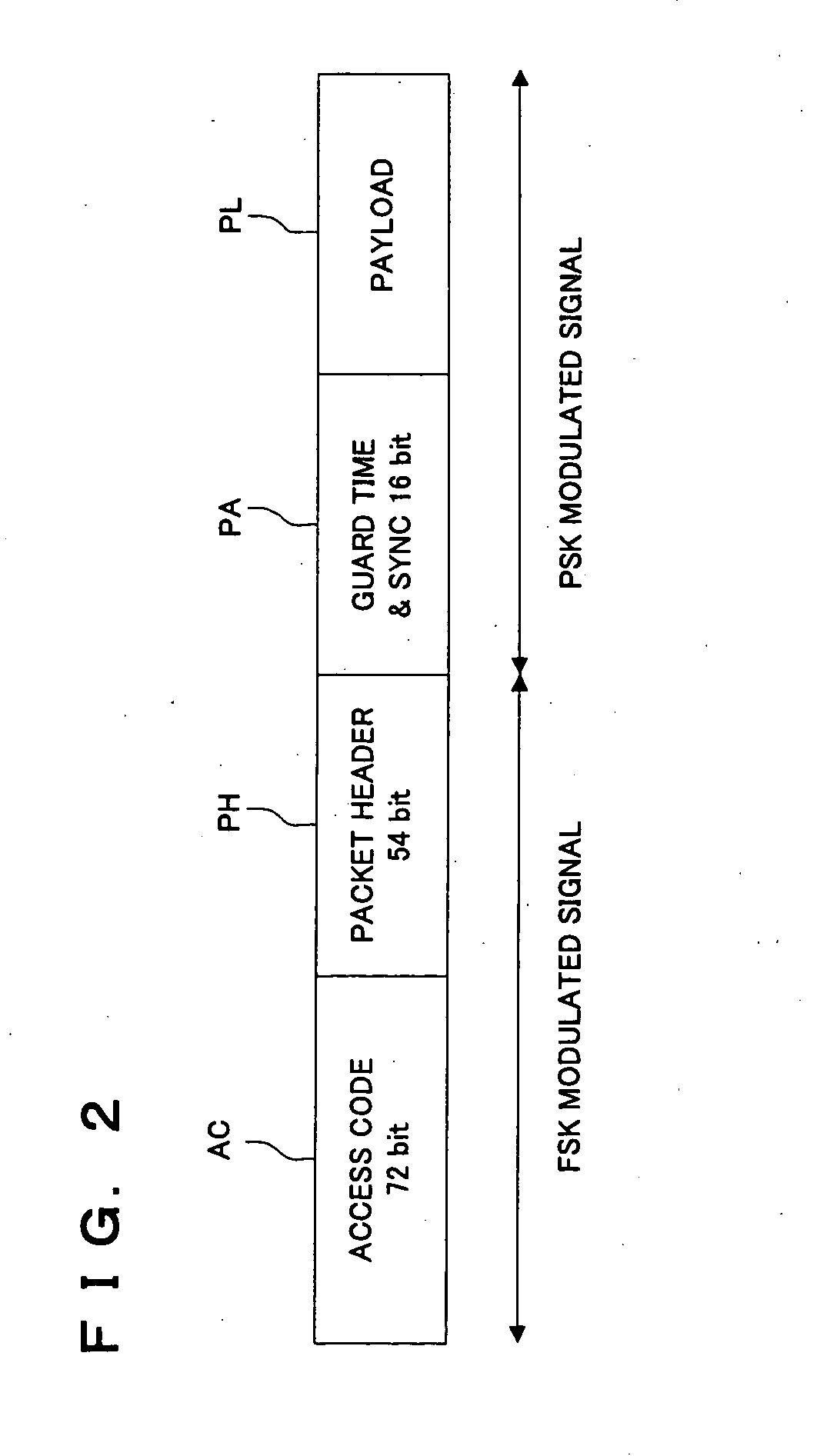
[0040] Here, as shown in FIG. 2, a format of the transmission packet to be sent on the transmission sid...
second embodiment
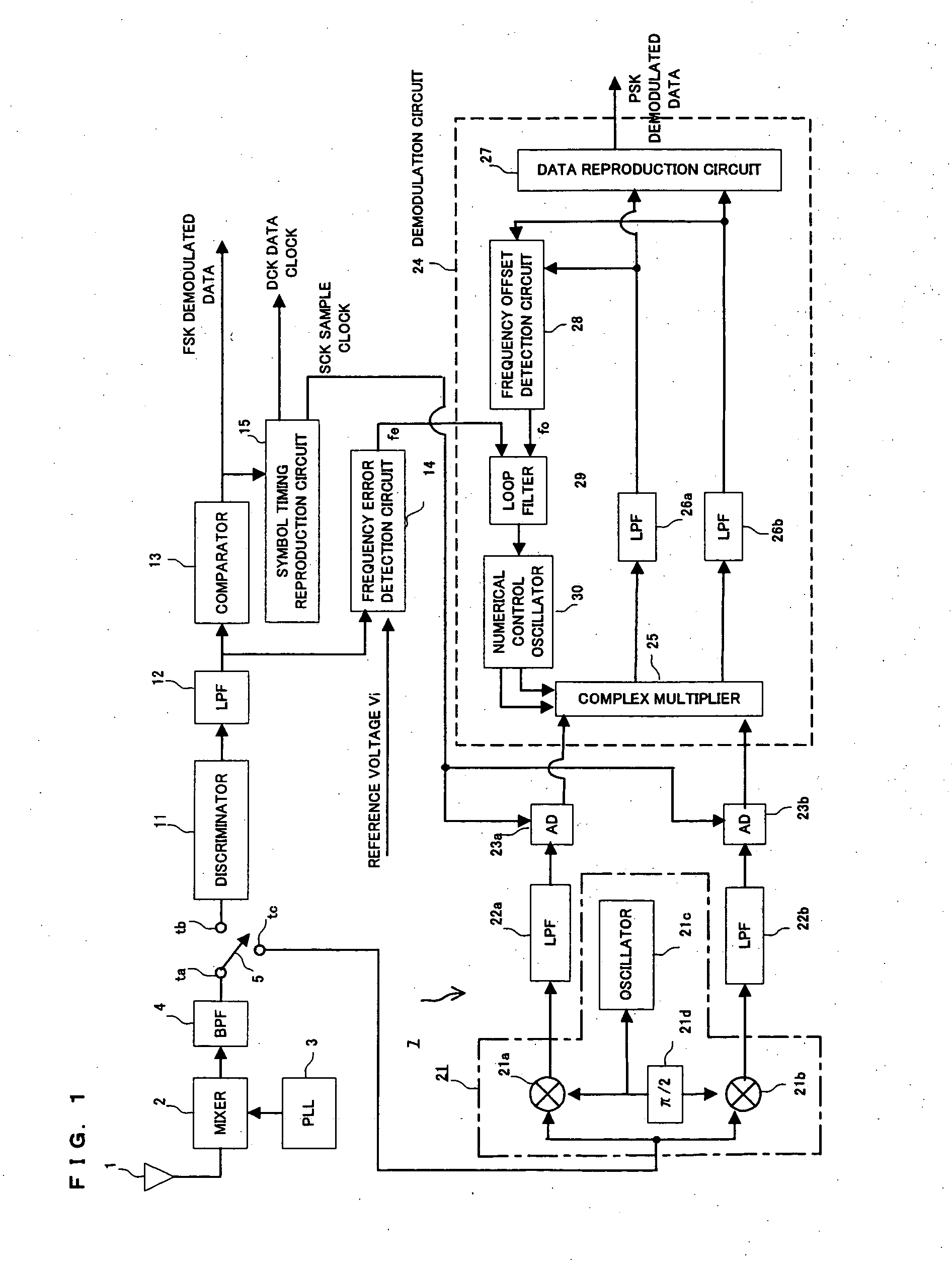
[0065] Next, the present invention will be described about FIG. 7.
[0066] This second embodiment is adapted to constitute the demodulation circuit 24 of the PSK demodulation unit 7 in the first embodiment using a phase angle calculator.
[0067] In other words, as shown in FIG. 7, the second embodiment has the same structure as FIG. 1 except that the demodulation circuit 24 in the first embodiment is changed to the demodulation circuit 40 which uses a phase angle calculator. Components corresponding to those in FIG. 1 are denoted by the identical numerals and signs, and a detailed description of the components is omitted.
[0068] The demodulation circuit 40 includes: an angle calculator 41 to which digital signals, which are outputted from the A / D converters 23a and 23b, are inputted; a phase locked loop (PLL) circuit 42 to which phase information, which is outputted from this angle calculator 41, is inputted; and a judgment circuit 43 which decodes phase information, which is formed by...
PUM
 Abstract
Description
Claims
Application Information
 - Generate Ideas
- Intellectual Property
- Life Sciences
- Materials
- Tech Scout
- Unparalleled Data Quality
- Higher Quality Content
- 60% Fewer Hallucinations
Browse by: Latest US Patents, China's latest patents, Technical Efficacy Thesaurus, Application Domain, Technology Topic, Popular Technical Reports.
© 2025 PatSnap. All rights reserved.Legal|Privacy policy|Modern Slavery Act Transparency Statement|Sitemap|About US| Contact US: help@patsnap.com