Single-substrate-heat-processing apparatus for performing reformation and crystallization

a technology of single substrate and crystallization, which is applied in the direction of coatings, chemical vapor deposition coatings, capacitors, etc., can solve the problems of reducing through-put, and increasing so as to reduce facility cost and manufacturing cost, and increase through-put

Inactive Publication Date: 2005-01-27
TOKYO ELECTRON LTD
View PDF15 Cites 48 Cited by
  • Summary
  • Abstract
  • Description
  • Claims
  • Application Information

AI Technical Summary

Benefits of technology

[0010] An object of the present invention is to provide a single-substrate-heat-processing apparatus and method for performing a reforming process and a crystallizing process while increasing the through-put and reducing the facility cost and the manufacturing cost.

Problems solved by technology

However, the number of the process steps and the number of transfer steps are increased in this prior art, leading to a decrease in the through-put.
In addition, the facility cost and the manufacturing cost are increased.

Method used


Image

  • Single-substrate-heat-processing apparatus for performing reformation and crystallization
  • Single-substrate-heat-processing apparatus for performing reformation and crystallization
  • Single-substrate-heat-processing apparatus for performing reformation and crystallization

Examples


Embodiment Construction

[0062] Embodiments of the present invention will be described hereinafter with reference to the accompanying drawings. In the following description, the constituent elements having substantially the same function and arrangement are denoted by the same reference numerals, and a repetitive description will be made only when necessary.

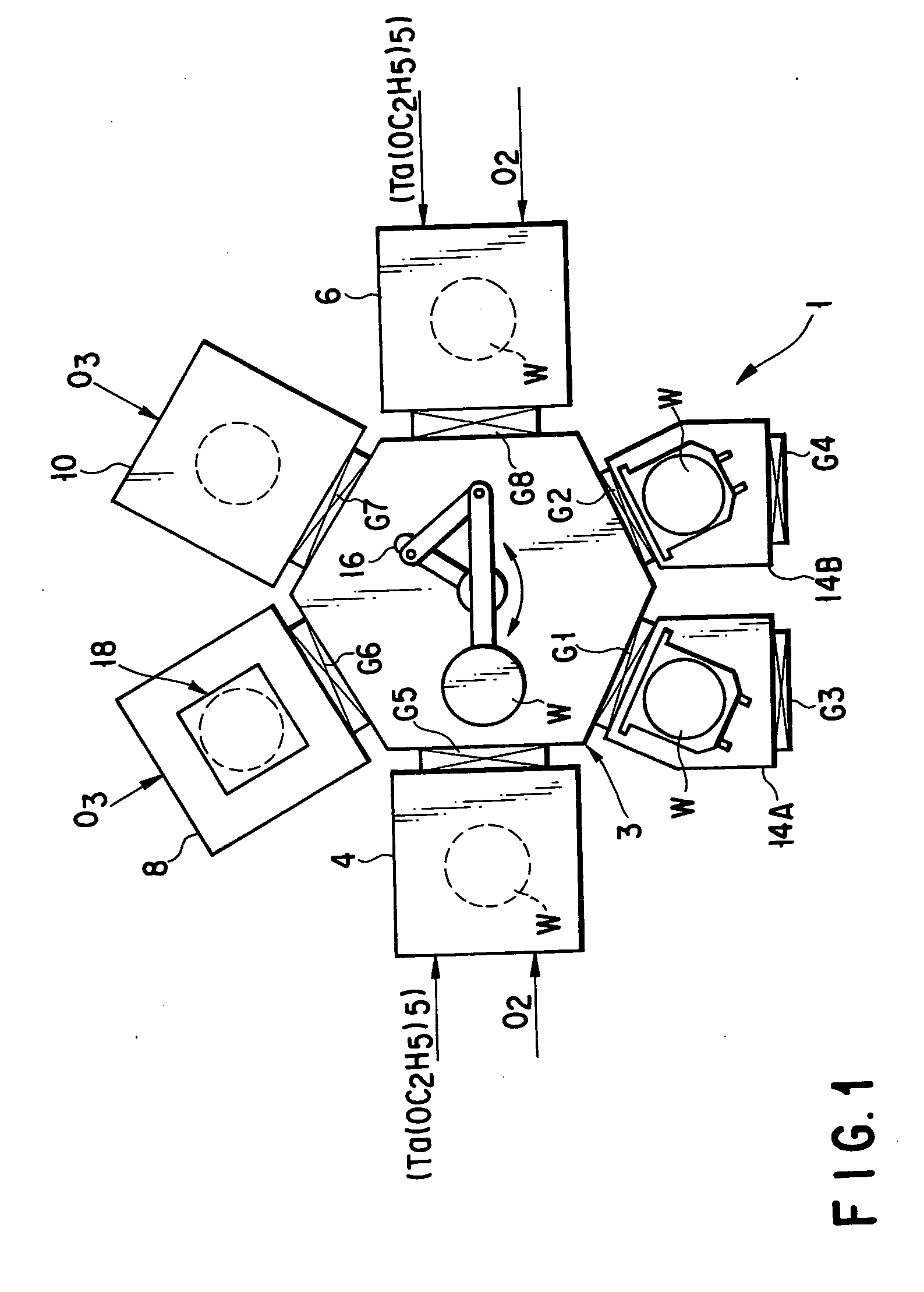
[0063]FIG. 1 schematically shows the constitution of the main part of a cluster-tool-type film forming system 1 according to one embodiment of the present invention.

[0064] In the film forming system 1 shown in FIG. 1, two CVD apparatuses 4 and 6, a reforming apparatus 8 and a heat processing apparatus 10 are connected to a common transfer chamber 3. Further, two cassette chambers 14A and 14B are also connected to the common transfer chamber 3 for improving the wafer transfer efficiency. A wafer is transferred among these apparatuses 4, 6, 8, 10 and the cassette chambers 14A, 14B through the common transfer chamber 3. For transferring the wafer, an arm ...


PUM

PropertyMeasurementUnit
wavelengthaaaaaaaaaa
temperatureaaaaaaaaaa
thickness t1aaaaaaaaaa

Abstract

An insulating film consisting of first and second tantalum oxide layers is formed on a semiconductor wafer. First, an amorphous first layer is formed by CVD, and a reforming process for removing organic impurities contained in the first layer is carried out. Then, an amorphous second layer is formed by CVD on the first layer. Then, a reforming process for removing organic impurities contained in the second layer is carried out by supplying a process gas containing ozone into a process chamber while heating the wafer to a temperature lower than a crystallizing temperature over a certain period. Further, within the same process chamber, the wafer is successively heated to a second temperature higher than the crystallizing temperature, followed by cooling the wafer to a temperature lower than the crystallizing temperature so as to crystallize the first and second layers simultaneously.

Description

BACKGROUND OF THE INVENTION [0001] The present invention relates to a single-substrate-heat-processing apparatus and method for performing a reforming process for removing inorganic impurities contained in a thin film formed on a target substrate and for performing a crystallizing process for crystallizing the thin film, and particularly, to a heat processing apparatus and method applied to a metal oxide film deposited by MOCVD (Metal Organic Chemical vapor Deposition) method. [0002] In the manufacturing process of a semiconductor device, a film forming process and a pattern etching process are repeatedly applied to a semiconductor wafer. The specification for the film forming process becomes severer and severer in recent years in accordance with increases in the density and in the degree of integration of the semiconductor devices. For example, a further a decrease in thickness and a higher insulating properties are required even for a very thin insulating film such as an insulatin...

Claims


Application Information

Patent Timeline
Patent Type & Authority Applications(United States)
IPC IPC(8): C23C16/44C23C16/56H01L21/02H01L21/316
CPCC23C16/405C23C16/44H01L28/56H01L21/31604C23C16/56H01L21/02183H01L21/02271H01L21/02356H01L21/02348H01L21/0234
Inventor SHINRIKI, HIROSHISUGIURA, MASAHITO
Owner TOKYO ELECTRON LTD
Why Eureka
Try Eureka