

Wiring substrate for intermediate connection and multi-layered wiring board and their production
- Summary
- Abstract
- Description
- Claims
- Application Information
AI Technical Summary
Benefits of technology
Problems solved by technology
Method used
Image

Examples
embodiment 1
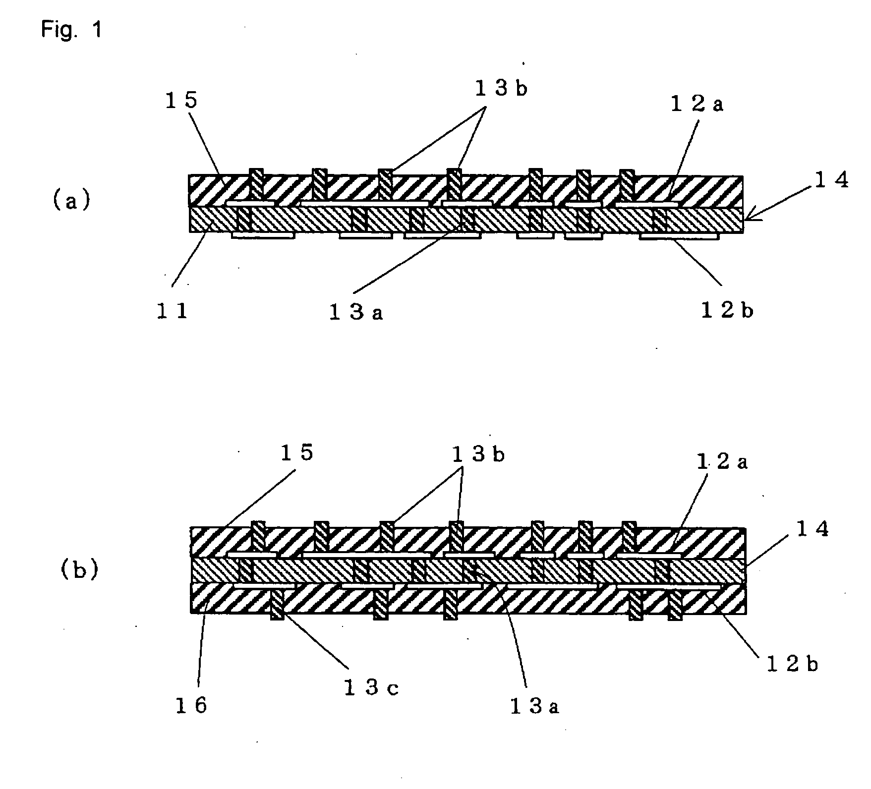
[0061] Embodiment 1
[0062] FIGS. 1(a) and 1(b) each schematically shows as embodiment 1 a wiring substrate for intermediate connection of the present invention. In FIG. 1(a), the wiring substrate for intermediate connection is configured such that a prepreg sheet 15 (having a thickness of for example less than 50 μm) which has via holes filled with a conductive paste 13b in a semi-cured condition is bonded to one surface (top surface in the shown embodiment) of a double-sided wiring board 14 which comprises an insulation layer 11 (having a thickness of for example less than 50 μm) having a first wiring layer 12a and a second wiring layer 12b on either side thereof respectively which are formed of metal foils (such as a copper foil) and which are connected as predetermined with via hole conductors (already cured) 13a containing copper powder as a dominant conductive component. Such bonding is carried out by thermo-compression at a temperature at which curing of the thermoset resin of ...
embodiment 2
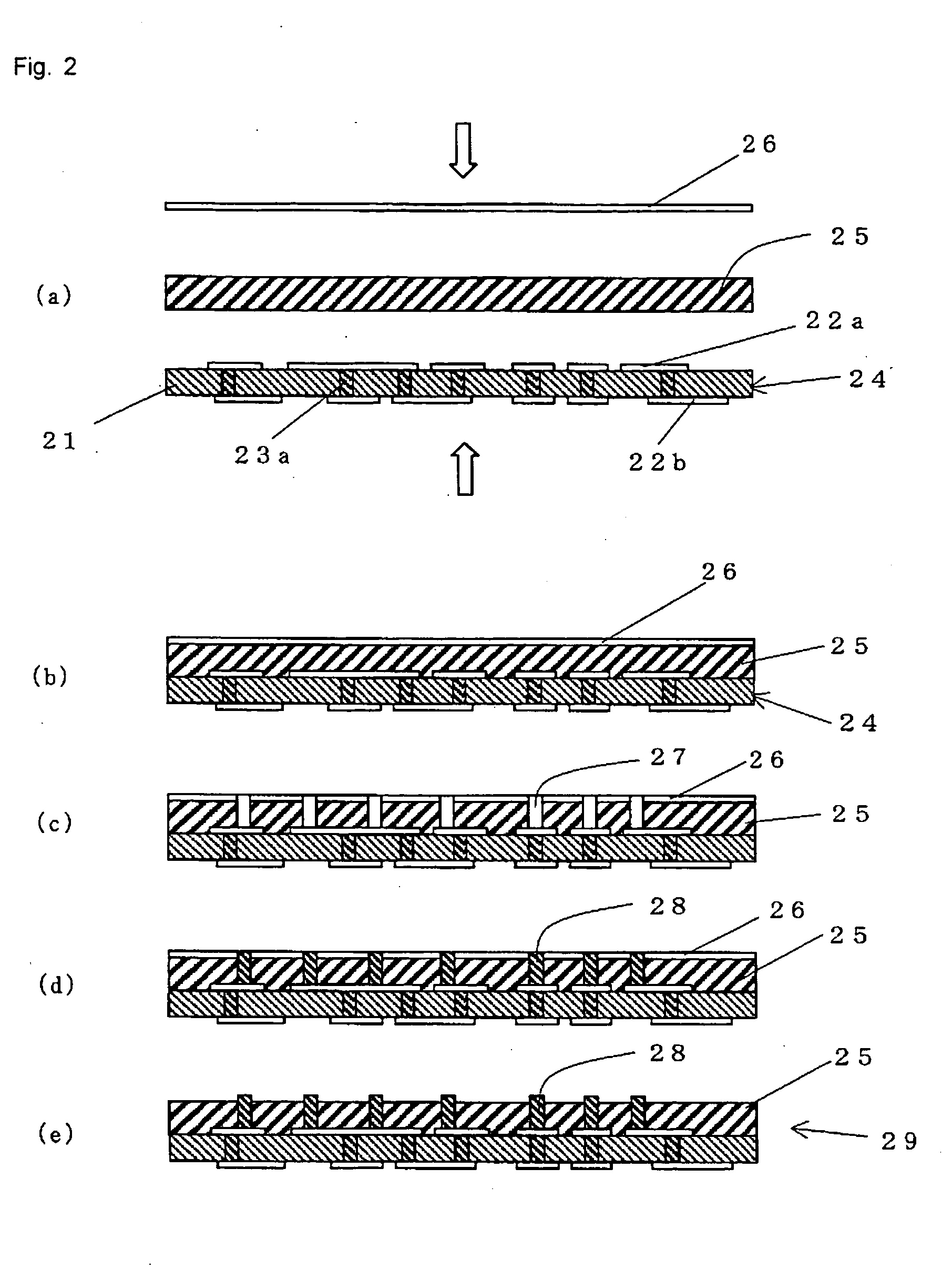
[0068] Embodiment 2
[0069] A production process of the wiring substrate for intermediate connection of the present invention is explained with reference to FIG. 2. FIGS. 2(a) to 2(e) each shows in a cross sectional view a step of the manufacturing process of the wiring substrate for intermediate connection of the present invention. As shown in FIG. 2(a), a prepreg sheet 25 (for example, a prepreg sheet in which a thermoset resin such as an epoxy resin is impregnated in the fibrous sheet of an aramid fiber unwoven fabric, and the resin is kept in the semi-cured condition (that is, in the B-stage condition)) is stacked on a double-sided wiring board 24 in which a first wiring layer 22a and a second wiring layer 22b installed on either side of the insulating layer 21 are connected through the via hole conductors 23a, and a release film 26 (for example, a release film made of a polyethylene terephthalate) having a thickness of about 20 micrometers is stacked on the prepreg sheet 25. Then...
embodiment 3
[0076] Embodiment 3
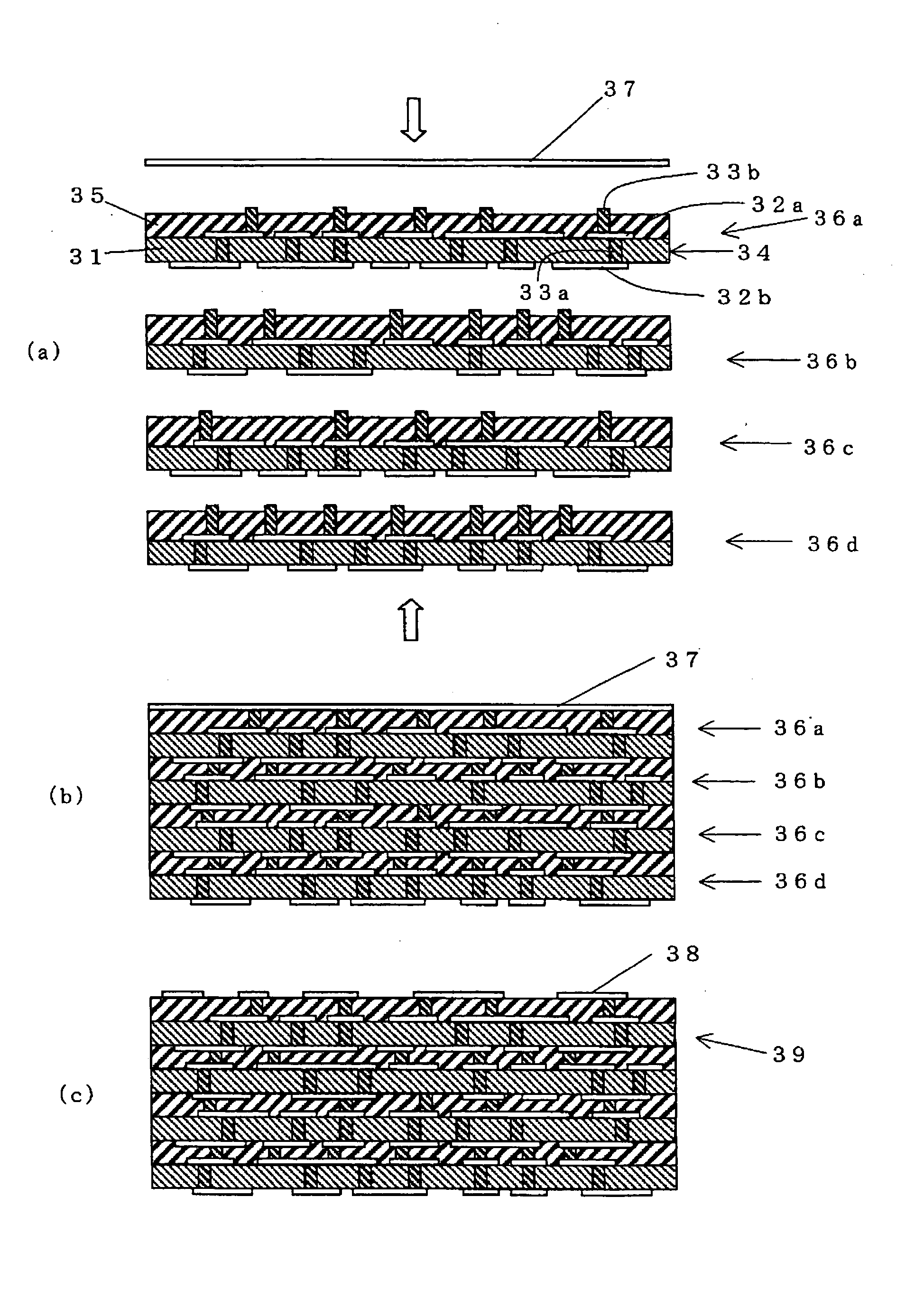
[0077] The multi-layered wiring board of the present invention and its production process of embodiment 3 are explained referring to FIG. 3. This embodiment produces the multi-layered wiring board with using the wiring substrate for intermediate connection which is described in the above embodiments 1 and 2.
[0078] FIGS. 3(a) to, 3(c) each shows a step for the production process of the multi-layered wiring board in the present embodiment. The wiring substrate for intermediate connection 36a as shown in FIG. 1(a) (which is formed by laminating a prepreg sheet 35 having via hole conductors 33b in the semi-cured condition onto one surface of a double-sided wiring board 34 having a first wiring layer 32a and a second wiring layer 32b on both sides of an insulation layer 31 which are connected with via hole conductors 33a is stacked together and aligned with similar wiring substrates for intermediate connection 36b, 36c and 36d which may be the same or different from e...
PUM
| Property | Measurement | Unit |
|---|---|---|
| Thickness | aaaaa | aaaaa |
| Diameter | aaaaa | aaaaa |
| Flexibility | aaaaa | aaaaa |
Abstract
Description
Claims
Application Information