Ceramic heater

a ceramic heater and heater body technology, applied in the field of ceramic heaters, can solve the problems of short circuit, inability to use ceramics, and inability to control the temperature of ceramics,

Inactive Publication Date: 2005-01-27
IBIDEN CO LTD
View PDF89 Cites 5 Cited by
  • Summary
  • Abstract
  • Description
  • Claims
  • Application Information

AI Technical Summary

Benefits of technology

[0128] By letting the ceramic substrate warp in one direction in this way, in case that a semiconductor wafer is heated in the state that the semiconductor wafer is separated from the ceramic substrate by a given distance, the distance between the semiconductor wafer and the ceramic substrate can easily be grasped and the surface temperature of the semiconductor wafer can be made even.

Problems solved by technology

Therefore, even if resistance heating elements are disposed on the surface of such a conductive carbide ceramic, a short circuit is caused between circuits so that the temperature thereof cannot be controlled.
However, even if circuits are formed on such a ceramic, a short circuit is caused.
Therefore, the ceramic cannot be used, as it is, as a ceramic substrate.
Furthermore, a ceramic comprising a nitride and the like which has insulation at ambient temperature has defects such as oxygen forming solid-solution.
This causes a drop in volume resistivity at high temperature to result in a problem that a short circuit is caused between circuits, thus making temperature-control impossible.
On the other hand, particularly when a semiconductor wafer is heated in the state that the semiconductor wafer and a ceramic substrate are separated from each other, a phenomenon that the temperature of the semiconductor wafer becomes uneven is observed even though the temperature of the surface of the ceramic substrate is made even.

Method used


Image

  • Ceramic heater
  • Ceramic heater
  • Ceramic heater

Examples


example 1

Production of a Ceramic Heater Made of Silicon Carbide

[0135] (1) The following were mixed: 100 parts by weight of silicon carbide powder (average particle diameter: 0.3 μm), 4 parts by weight of B4C (average particle diameter: 0.5 μm) as a sintering aid, 0.5 part by weight of C (Mitsubishi Diablack, made by Mitsubishi Chemical Corp.), 12 parts by weight of an acrylic binder, 0.5 part by weight of a dispersant and an alcohol. Thereafter, the mixture was subjected to spray-drying to make granular powder.

[0136] (2) Next, this granular powder was put into a mold and formed into a flat plate form to obtain a raw formed body (green).

[0137] (3) The raw formed body subjected to the above-mentioned processing treatment was hot-pressed at 2100° C. and a pressure of 17.6 (180 kg / cm2) MPa to obtain a silicon carbide ceramic substrate having a thickness of 3 mm.

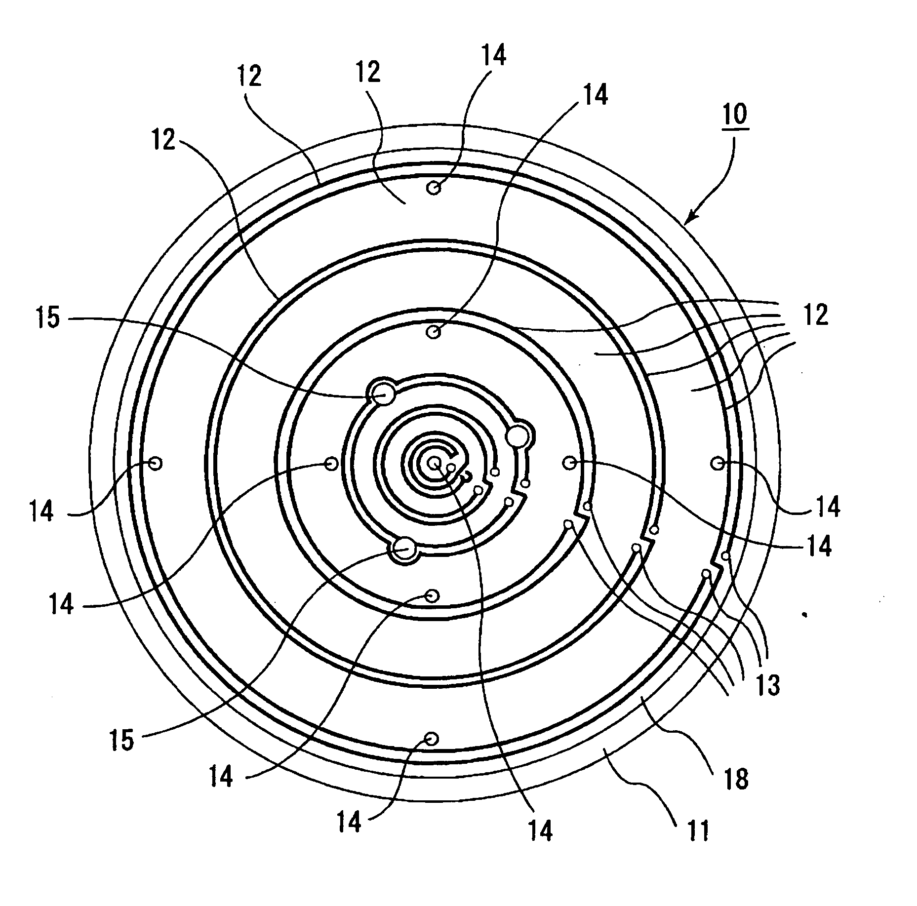
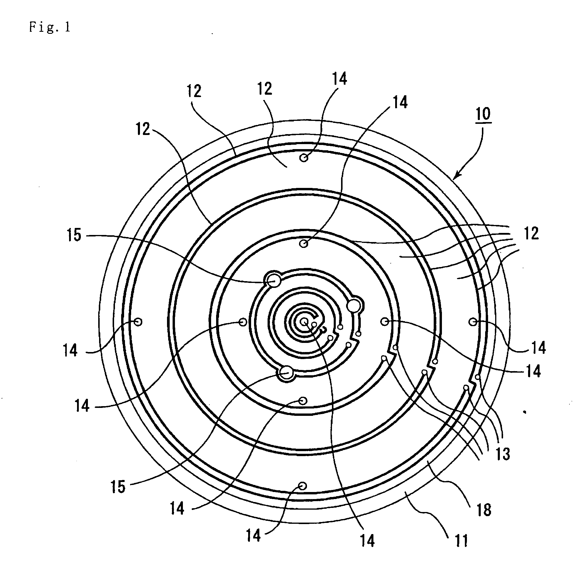
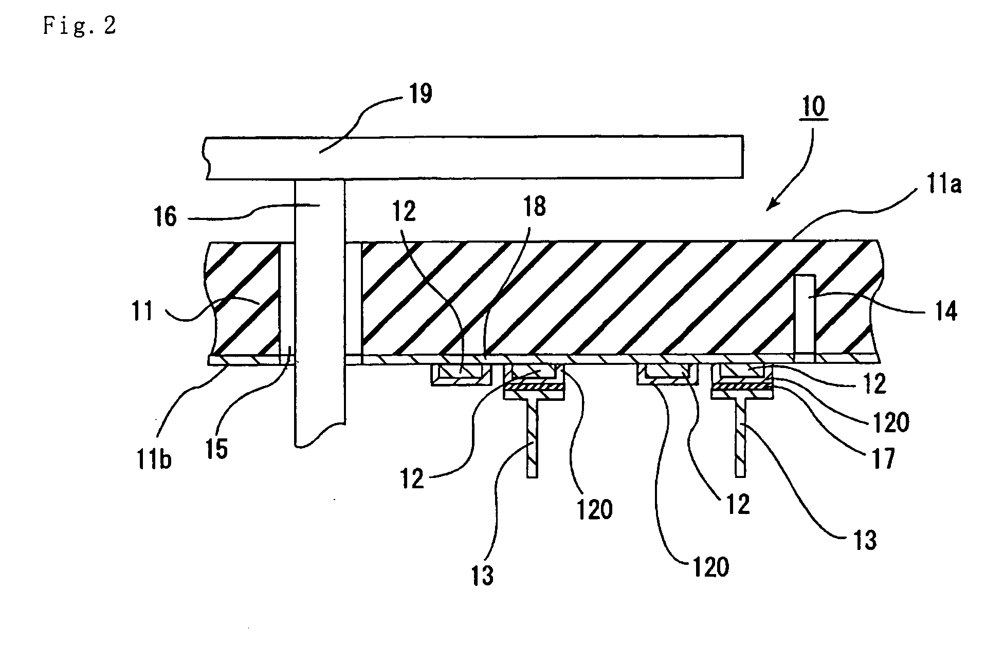
[0138] Next, this plate was cut out into a disk having a diameter of 210 mm to prepare a ceramic substrate 11.

[0139] (4) Next, a so...

example 2

Production of a Ceramic Heater Made of Silicon Carbide

[0148] A ceramic heater made of silicon carbide was produced in the same manner as in Example 1 except that powder of silicon carbide having an average particle diameter of 1.0 μm was used, the sintering temperature was set to 1900° C., and further the surface of the resultant ceramic substrate was fired at 1500° C. for 2 hours to form an insulating layer having a thickness of 1 μm and comprising SiO2.

example 3

Production of a Ceramic Heater Made of Aluminum Nitride

[0149] (1) A composition made of 100 parts by weight of aluminum nitride powder (average particle diameter: 0.6 μm), 4 parts by weight of yttria (Y2O3, average particle diameter: 0.4 μm), 12 parts by weight of an acrylic resin binder, and an alcohol was subjected to spray-drying , so as to make granular powder.

[0150] (2) Next, this granular powder was put into a mold and formed into a flat plate form to obtain a raw formed body (green).

[0151] (3) The raw formed body subjected to the above-mentioned processing treatment was hot-pressed at 1800° C. and a pressure of 200 kg / cm2 to obtain an aluminum nitride sintered body having a thickness of 3 mm.

[0152] Next, this plate was cut out into a disk having a diameter of 210 mm to prepare a ceramic substrate 11. In the same way as in Example 1, the sol solution used in Example 1 was applied onto the bottom face of this ceramic substrate, and the resultant product was dried and fired,...


PUM

PropertyMeasurementUnit
thicknessaaaaaaaaaa
thicknessaaaaaaaaaa
thicknessaaaaaaaaaa

Abstract

An objective of the present invention is to provide a ceramic heater making it possible to prevent a short circuit in its resistance heating element and heat a semiconductor wafer evenly. The ceramic heater of the present invention is a ceramic heater comprising: a ceramic substrate; an insulating layer having volume resistivity higher than that of said ceramic substrate, being formed on at least a part of said ceramic substrate; and a resistance heating element formed on said insulating layer.

Description

FIELD OF THE INVENTION [0001] The present invention relates to a ceramic heater which is used mainly in the semiconductor industry, particularly to a ceramic heater superior in insulation between circuits of resistance heating elements. BACKGROUND ART [0002] Semiconductors are very important goods necessary in various industries. A semiconductor chip, which is a typical product thereof, is produced, for example, by slicing a silicon monocrystal into a given thickness to produce a silicon wafer, and then forming various integrated circuits and the like on this silicon wafer. [0003] In order to form integrated circuits and so on of this type, it is necessary to conduct a process of applying a photosensitive resin onto the silicon wafer, exposing the resin to light, developing the exposed resin and then subjecting the resultant to post-curing and sputtering, to form a conductor layer. For this purpose, it is necessary to heat the silicon wafer. [0004] As this heater for heating the sil...

Claims


Application Information

Patent Timeline
Patent Type & Authority Applications(United States)
IPC IPC(8): H01L21/00H05B3/14H05B3/26
CPCH01L21/67103H05B3/265H05B3/143
Inventor HIRAMATSU, YASUJI
Owner IBIDEN CO LTD
Why Eureka
Try Eureka