Semiconductor device and fabrication method thereof

a technology of semiconductor devices and semiconductor elements, applied in semiconductor devices, semiconductor/solid-state device details, electrical apparatus, etc., can solve the problems of limiting the relationship between the upper layer semiconductor element, and the outer size of the lower layer semiconductor element must be larger, so as to increase the filing ratio of the sealing resin and the viscosity of the sealing resin

Inactive Publication Date: 2005-01-27
SONY CORP
View PDF5 Cites 13 Cited by
  • Summary
  • Abstract
  • Description
  • Claims
  • Application Information

AI Technical Summary

Benefits of technology

[0019] With this configuration, since the viscosity of the sealing resin is lower than the viscosity of the resin used for forming the resin peripheral wall, it is possible to increase a filing ratio of the sealing resin in the space of the resin peripheral wall

Problems solved by technology

The related art semiconductor device 1 shown in FIG. 4, however, has an inconvenience that an outer size of the lower layer semiconductor element must be larger than an electrode area, in which electrodes are disposed, of the upper layer semiconductor element.
If such a support is not provided (that is, in an overhang state), when the bonding wire is connected to each electrode of the upper layer semiconductor element, a mechanical load is partially applied to the upper layer semiconductor element, res

Method used


Image

  • Semiconductor device and fabrication method thereof
  • Semiconductor device and fabrication method thereof
  • Semiconductor device and fabrication method thereof

Examples


Embodiment Construction

[0025] Hereinafter, preferred embodiments of a semiconductor device and a semiconductor device structure will be described in detail with reference to the drawings.

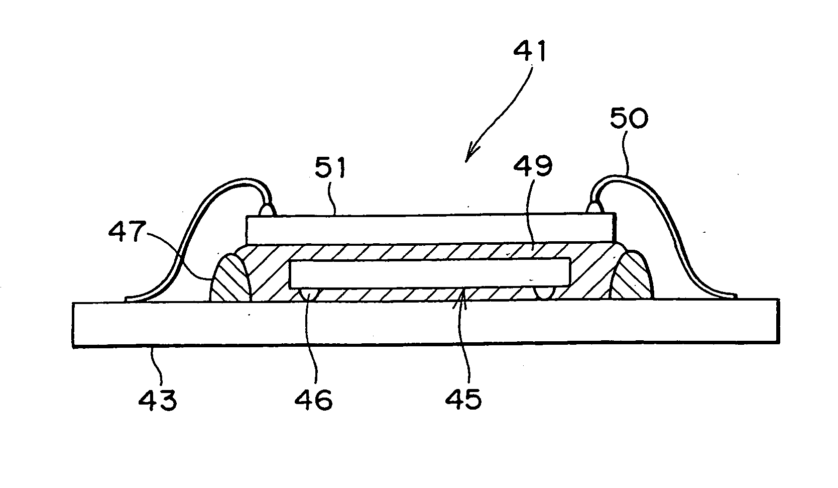
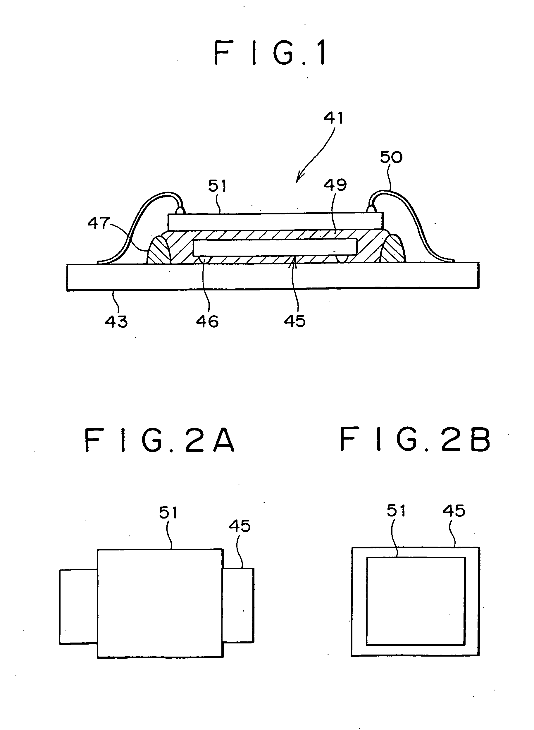
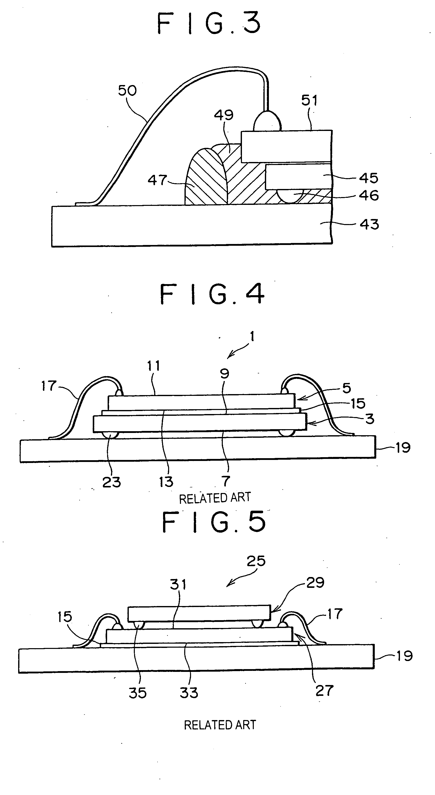
[0026]FIG. 1 is a sectional view of a semiconductor device of the present invention; FIGS. 2A and 2B are views each illustrating a combination example of outer sizes of semiconductor elements; and FIG. 3 is an enlarged sectional view of an essential portion of a modification of the semiconductor device shown in FIG. 1.

[0027] In a semiconductor device 41 according to this embodiment, a first semiconductor element (lower layer semiconductor element) 45 is bonded, in a flip-chip bonding manner, to a wiring board 43 by means of bumps 46. A resin peripheral wall 47 is formed on the wiring board 43 in such a manner as to surround the first semiconductor element 45. The shape of the resin peripheral wall 47 is determined by an electrode area of a second semiconductor element (which will be described later). In other words, the...


PUM


Abstract

The present invention provides a semiconductor device including a first semiconductor element to be bonded to a wiring board in a flip-chip bonding manner, a resin peripheral wall provided on the wiring board in such a manner as to surround the first semiconductor element, a sealing resin poured so as to fill a space surrounded by the resin peripheral wall and then hardened, and a second semiconductor element provided in such a manner that a back surface thereof is fixed on an upper surface of the sealing resin and a electrode provided on a front surface thereof is connected to a segment of wiring on the wiring board by means of a bonding wire, and provides a method of fabricating the semiconductor device. With this configuration, since semiconductor elements of arbitrary outer sizes can be stacked to each other without any limitation by the outer sizes of the semiconductor elements, even in a combination of any outer shapes of semiconductor elements vertically stacked to each other, the semiconductor elements can be mounted at a high density.

Description

BACKGROUND OF THE INVENTION [0001] The present invention relates to a semiconductor device including a plurality of semiconductor elements stacked to each other and a method of fabricating the semiconductor device, and particularly to a technique capable of stacking semiconductor elements to each other without any limitation by outer sizes of the semiconductor elements. [0002] If one semiconductor element is mounted on a wiring board, then an area of the wiring board is occupied with the semiconductor device, and thereby another semiconductor element is no longer mounted on the wiring board. On the other hand, in recent years, electronic devices such as video cameras, CDs, and cellular phones have been required to be further reduced in size and further enhanced in performance. To meet such a requirement, there has been proposed a semiconductor device, in which a semiconductor element mounting area becomes twice that of a prior art semiconductor device although the semiconductor devi...

Claims


Application Information

Patent Timeline
IPC IPC(8): H01L23/28H01L21/52H01L21/56H01L21/60H01L23/31H01L23/52H01L25/065H01L25/07H01L25/18
CPCH01L23/3135H01L24/48H01L25/0657H01L2224/16145H01L2224/16225H01L2224/16227H01L2224/27013H01L2224/32145H01L2224/32225H01L2224/48091H01L2224/48225H01L2224/48227H01L2224/48465H01L2224/73265H01L2224/83051H01L2225/0651H01L2225/06517H01L2225/06555H01L2225/06582H01L2924/01004H01L2924/01005H01L2924/01047H01L2224/73204H01L2924/01033H01L24/32H01L2924/00014H01L2924/00012H01L2924/00011H01L2924/00H01L24/73H01L2224/05599H01L2224/45099H01L2224/85399H01L2224/45015H01L2924/207H01L23/52
Inventor SHIBUE, HITOSHI
Owner SONY CORP
Why Eureka
Try Eureka