

Method of making photomask blank substrates
a technology of substrates and photomasks, applied in the field of making substrates for photomask blanks, can solve the problems of the accuracy of the photolithographic process employed in semiconductor manufacturing, and the inability to ignore the flatness of the substrate as a cause of focal shift, so as to reduce the minimum feature size and high accuracy
- Summary
- Abstract
- Description
- Claims
- Application Information
AI Technical Summary
Benefits of technology
Problems solved by technology
Method used
Image

Examples
example 1
[0091] A 152 mm (6 inch) square starting substrate for a photomask blank was polished with colloidal silica on a double side polishing machine at a higher polishing speed in the center of the substrate surface than at the periphery, giving a polished intermediate product which had, as shown in FIG. 5A, a principal surface region with a concave shape. Specifically, in the principal surface region, the difference between the maximum and minimum values for height from the principal surface-region least squares plane to the principal surface region (which difference is referred to hereinafter as the “principal surface flatness”) was 0.74 μm, and the difference between the maximum and minimum values for height from the principal surface-region least squares plane to the four corners of the principal surface region (CIR) was 0.27 μm.
[0092] Here and below, the principal surface flatness and the CIR were calculated from measurements of height obtained with a flatness tester at intervals of...
example 2
[0098] A 152 mm (6 inch) square starting substrate for a photomask blank was polished in the same way as in Example 1 at a higher polishing speed in the center of the substrate surface than at the periphery, giving a polished intermediate product which had, as shown in FIG. 6A, a principal surface region of concave shape. The principal surface flatness was 0.88 μm and the CIR was 0.27 μm.
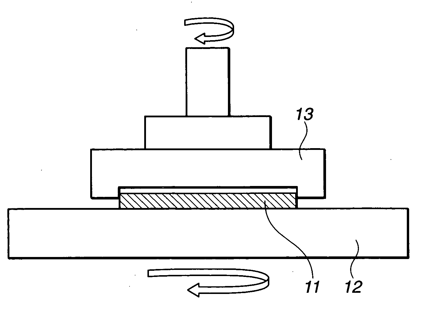
[0099] The polished intermediate product was then polished with colloidal silica, this time on a single side polishing machine like that shown in FIG. 4 having a polishing cloth fixed to the lower plate and at a lower polishing speed in the center of the substrate surface than at the periphery. [0100] Speed of reticle-holding plate: 120 rpm [0101] Speed of lower plate: 33 rpm [0102] Polishing time: 4 minutes
[0103] The resulting substrate (thickness, 6.4 mm) had, as shown in FIG. 6B, a principal surface region with a principal surface flatness of 0.27 μm and a CIR of 0.14 μm, and a quadrangular rin...
example 3
[0104] A 152 mm (6 inch) square starting substrate for a photomask blank was polished in the same way as in Example 1 at a higher polishing speed in the center of the substrate surface than at the periphery, giving a polished intermediate product which had, as shown in FIG. 7A, a principal surface region of concave shape. The principal surface flatness was 0.88 μm and the CIR was 0.52 μm.
[0105] The polished intermediate product was then polished with colloidal silica, this time on a single side polishing machine like that shown in FIG. 4 having a polishing cloth fixed to the lower plate and at a lower polishing speed in the center of the substrate surface than at the periphery. [0106] Speed of reticle-holding plate: 120 rpm [0107] Speed of lower plate: 50 rpm [0108] Polishing time: 7 minutes
[0109] The resulting substrate (thickness, 6.4 mm) had, as shown in FIG. 7B, a principal surface region with a principal surface flatness of 0.49 μm and a CIR of 0.41 μm, and strip-like regions...
PUM
| Property | Measurement | Unit |
|---|---|---|
| height | aaaaa | aaaaa |
| length | aaaaa | aaaaa |
| length | aaaaa | aaaaa |
Abstract
Description
Claims
Application Information