Flow sensor with self-aligned flow channel

a flow sensor and self-aligning technology, applied in the field of sensors, can solve the problems of unmet or met, flow sensors generally face potential degradation problems, expensive solutions, and frequent cleaning or replacement and recalibration of sensors, so as to reduce flow noise and potential corrosion, and improve electrical insulation

Inactive Publication Date: 2005-02-03
HONEYWELL INT INC
View PDF70 Cites 46 Cited by
  • Summary
  • Abstract
  • Description
  • Claims
  • Application Information

AI Technical Summary

Benefits of technology

[0015] A sensor can be configured to generally include a flow channel block having a flow channel formed therein. The sensor additionally includes a substrate fastened to a sensor chip and contacted by at least one bonding element and a molded core tube inserted into the flow channel of the flow channel block, which thereby reduces flow noise and potential corrosion, improves electrical insulation, structural integrity and thermal measurements thereof derived from the sensor chip.

Problems solved by technology

Such flow sensors generally face potential degradation problems when exposed to harsh (e.g., contaminated, dirty, condensing, etc.) fluids, including gases or liquids that can “stress” the sensor via corrosion, radioactive or bacterial contamination, overheating, deposits or freeze-ups.
The sensitive measurement of the flow, or pressure (differential or absolute) of “harsh” gases or liquids that can stress, corrode, freeze-up, or overheat the sensing elements is a challenge that is either unmet or met at great expense.
Frequent cleaning or replacement and recalibration of the sensors are additional, but costly, solutions.
Sensitive, membrane-based differential pressure sensors can be protected against contamination because no flow is involved, but they are less sensitive, typically cover a smaller flow range and are more expensive than thermal microsensors, in addition to not being overpressure proof.
The measurement of liquid flow via thermal microsensors, especially of electrically conductive fluids, thus presents challenging problems in terms of electrical insulation, flow noise, chip corrosion, potential for leaks or structural integrity of the flow channel, and thermal measurement.
Even potting the wire-bonds in highly cross-linked epoxy led to either resistances dropping to, for example, 30MΩ and / or bond breakage if the epoxy became too brittle due to excessive cross-linking and / or thermal cycling.
Additionally, an odd shape of the flow channel above the chip causes extra turbulence and corresponding signal noise.
Another approach to providing electrical insulation for the electrical contacts and leadout wires is to move them out of the fluid-flow channel and contact area; however, such sidewise displacement adds real estate to the chip size and therefore to its cost.
The resulting, relatively small signal causes more significant increases in the effect of composition-, sensor-material- and temperature-dependent offsets, which can cause significant errors in the sensor flow readouts.
Another challenge in the design and manufacture of flow sensors is the alignment of the fluid flow path across the sensing element.
Such precise alignment of sensors generally requires components of each sensor to be individually aligned, which is labor intensive and expensive.

Method used


Image

  • Flow sensor with self-aligned flow channel
  • Flow sensor with self-aligned flow channel
  • Flow sensor with self-aligned flow channel

Examples


Embodiment Construction

[0033] The particular values and configurations discussed in these non-limiting examples can be varied and are cited merely to illustrate various embodiments of the present invention and are not intended to limit the scope of the invention.

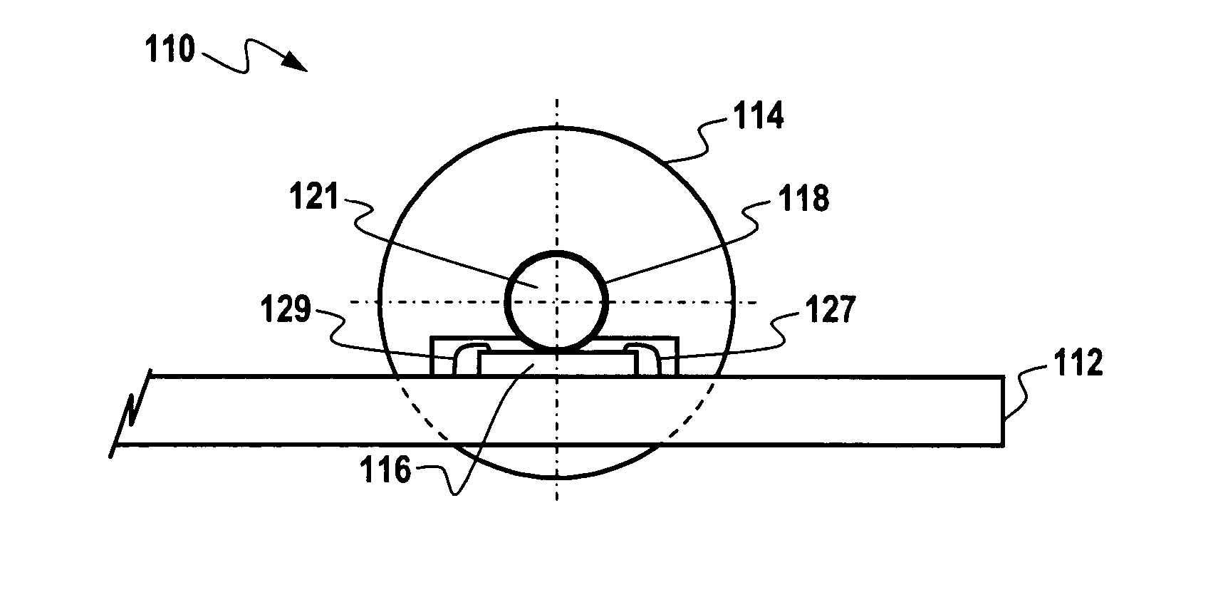
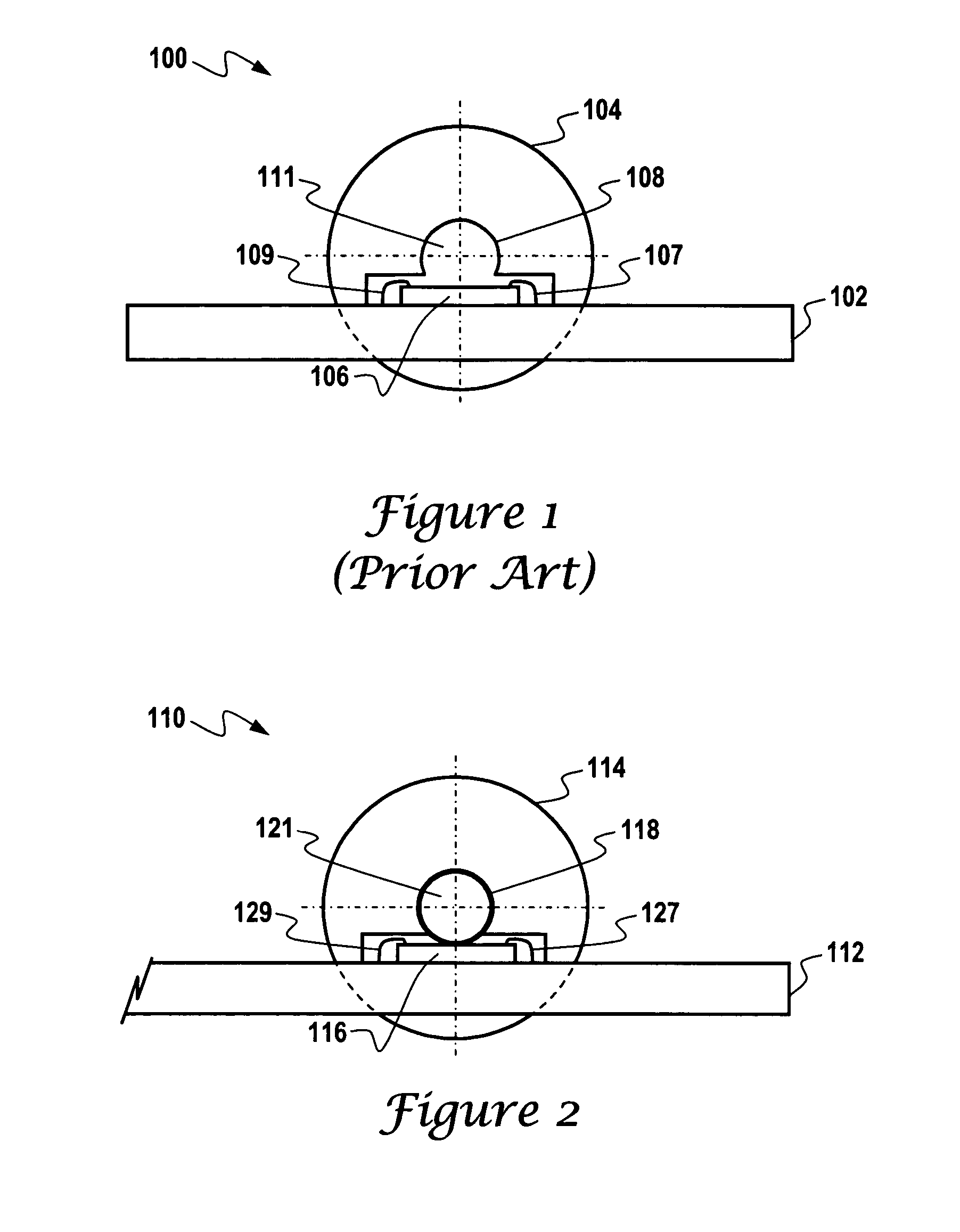
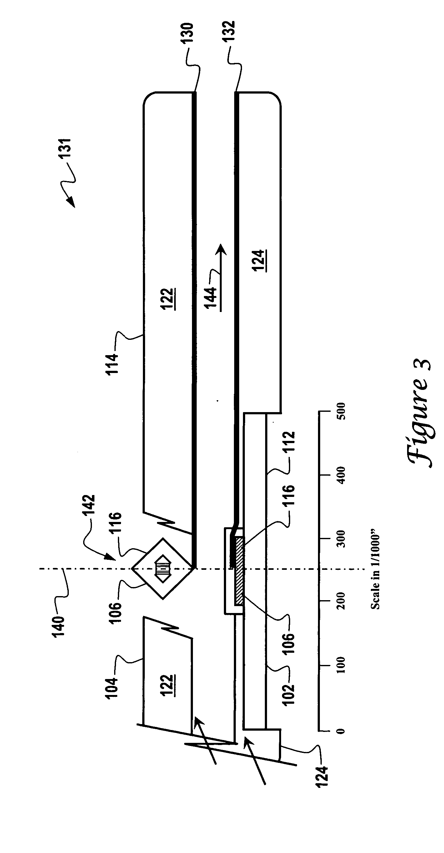
[0034] One aspect of the present invention is related to the design and fabrication of the electrical insulation for electrical contacts to sensor chips using either front-wire-bond (FWB) or through-the-wafer (TTW) contacts of certain thermal flow microsensors or of environmental sensors in general. The present inventors previously insulated Au-wires and Au-pads of FWB sensor chips via materials, such as, for example, dip-coatings, dip-coatings with or without alumina thin-film undercoating, Si3N4, flowable sealants, solvent-resistant sealant with fluoro-silicon, and epoxies. Insulation based on such materials has been attempted as defined generally by the resistances between the sensing elements and the liquid (e.g., salt water) in a flow tube. ...


PUM

PropertyMeasurementUnit
resistanceaaaaaaaaaa
resistancesaaaaaaaaaa
temperatureaaaaaaaaaa

Abstract

A flow sensor is provided having a substrate with a sensing element and flow channel aligned over the sensing element. The sensing element senses at least one property of a fluid. The flow channel is aligned by one or more guide elements formed in an alignment layer. The flow channel across the sensing area is accurately and precisely aligned due to the guide elements provided at the wafer-level, facilitating reliable, low-cost, and consistent results among multiple flow sensors. The flow sensor is adapted for use in harsh environments.

Description

[0001] This is a continuation-in-part of U.S. patent application Ser. No. 10 / 128,775, filed Apr. 22, 2002, entitled “Sensor Package for Harsh Environments”, which is a continuation-in-part of U.S. patent application Ser. No. 09 / 656,694, filed Sep. 7, 2000, entitled “Robust Fluid Flow and Property Microsensor Made of Optimal Material,” which is a continuation-in-part of U.S. patent application Ser. No. 09 / 207,165, filed Dec. 7, 1998, entitled “Rugged Fluid Flow and Property Microsensor,” now U.S. Pat. No. 6,184,773, and U.S. patent application Ser. No. 09 / 386,621, filed Aug. 5, 1999, which is a Continuation-in-Part of U.S. patent application Ser. No. 09 / 239,125, filed Jan. 28, 1999, both entitled “Microsensor Housing,” now U.S. Pat. Nos. 6,322,247 and 6,361,206 respectively. The content of the foregoing patent applications and patents are hereby incorporated by reference.FIELD OF THE INVENTION [0002] The present invention relates generally to sensors utilized to detect the quality an...

Claims


Application Information

Patent Timeline
Patent Type & Authority Applications(United States)
IPC IPC(8): G01F1/684G01F5/00G01N1/22G01N25/18G01N25/48G01N33/00
CPCG01F1/684Y10T29/49147G01F1/6845G01F1/6847G01F5/00G01F15/14G01F15/18G01F15/185G01N1/2247G01N25/18G01N25/488G01N33/0014G01N2001/2285Y10T29/49117Y10T29/49135Y10T29/49798Y10T29/4913G01F1/6842
Inventor PADMANABHAN, ARAVINDBONNE, ULRICHMARCHINI, MICHAEL G.
Owner HONEYWELL INT INC
Why Eureka
Try Eureka