Wafer edge defect inspection

a defect inspection and wafer edge technology, applied in the field of wafer defect inspection, can solve problems such as cracks in the wafer edge, large problems, and the possibility of propagation of cracks in the wafer to the interior of the wafer, and achieve the effect of greater consideration

Active Publication Date: 2005-02-03
BELL SEMICON LLC
View PDF5 Cites 73 Cited by
  • Summary
  • Abstract
  • Description
  • Claims
  • Application Information

AI Technical Summary

Benefits of technology

[0007] The present invention arose out of the recognition of the importance of wafer edge defects relative to yield rate and the need to give greater consideration to edge defects during wafer fabrication. It was realized that defects at the edge of a wafer, though they are far from the IC's on the surface of the wafer, frequently cause problems in the fabrication of the IC's. For instance, process-induced edge contamination and flaking from the wafer edge are types of defects that can cause considerable problems in IC fabrication, particularly when particles or flakes break off of the edge and land on the top surface of the wafer during a process step. Additionally, cracks i

Problems solved by technology

It was realized that defects at the edge of a wafer, though they are far from the IC's on the surface of the wafer, frequently cause problems in the fabrication of the IC's.
For instance, process-induced edge contamination and flaking from the wafer edge are types of defects that can cause considerable problems in IC fabrication, particularly when particles or flakes break off of the edge and land on the top surface of the wafer during a process step.
Additionally, cracks in the wafer edge may propagate to the interior of the wafer, particularly during process steps that thermally cycle the wafer.
Furthermore, with the introduction of new wafer processing technologies such as the use of low-K dielectric

Method used


Image

  • Wafer edge defect inspection
  • Wafer edge defect inspection
  • Wafer edge defect inspection

Examples


Embodiment Construction

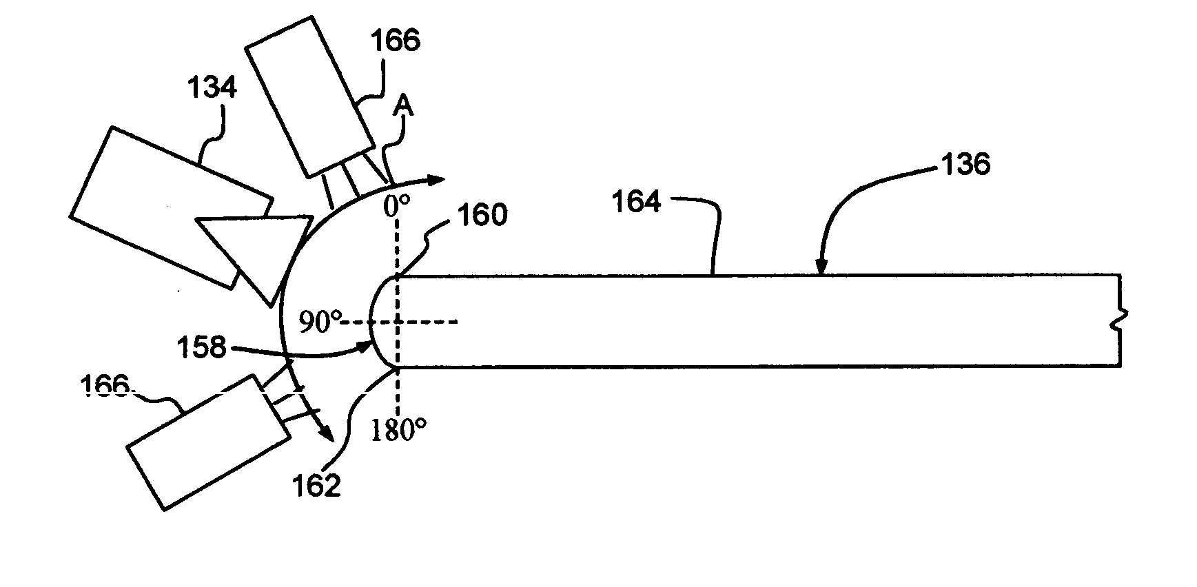
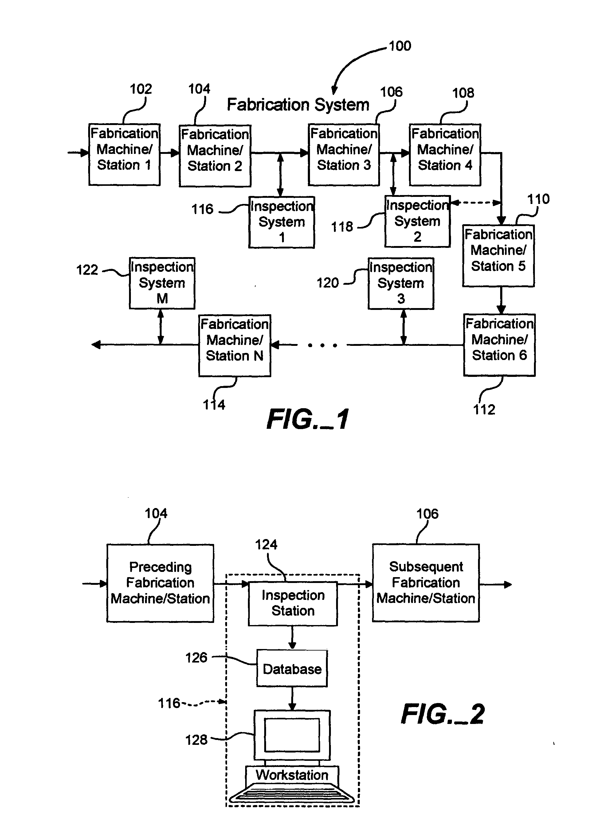
[0019] An exemplary fabrication system 100 that fabricates integrated circuits (IC's) (not shown) on semiconductor wafers (not shown) is shown in FIG. 1. The fabrication system 100 includes several conventional fabrication machines, or stations, 102-114, such as metal deposition devices, ion implantation devices, epitaxial growth chambers, ovens, spin-on-glass devices, etc. Thus, the fabrication stations 102-114 perform various conventional process steps in a specific processing order on the wafers in order to fabricate the IC's. The fabrication system 100 also includes inspection systems 116-122. Each inspection system 116-122 is interposed between two fabrication stations 102-114 to intercept one or more or all of the wafers passing between the fabrication stations 102-114 for inspection purposes. Each inspection system 116, 118, 120 and 122 corresponds to the fabrication station 104, 106, 112 and 114, respectively, that immediately precedes it in the processing order. The inspect...


PUM


Abstract

A wafer edge defect inspection method and apparatus for use in an integrated circuit fabrication system includes an image capturing device for capturing images of the edges of wafers, a database in which the images are stored and accessible for analysis and a computer for analyzing the images of one or more wafer edges to locate edge defects and for evaluating the performance of the fabrication system. The inspection and data storage are performed automatically. The database storage enables detailed analysis of many wafers and fabrication process steps.

Description

FIELD OF THE INVENTION [0001] This invention relates to wafer defect inspection within fabrication systems that form integrated circuits (ICs) on semiconductor wafers. In particular, this invention relates to new and improved techniques for inspecting the edges of the wafers for defects preferably between various process steps during the over-all fabrication of the wafers within the fabrication system. BACKGROUND OF THE INVENTION [0002] A significant trend throughout IC development has been to try to increase the “yield rate” of semiconductor fabrication systems. The yield rate refers to the percentage of usable IC's produced by a fabrication system compared to the total number attempted. Similarly, the yield rate may refer to the percentage of usable IC's obtained from an average semiconductor wafer that is processed through the fabrication system. A semiconductor wafer is essentially a thin disc of highly purified semiconductor material on which many IC's are fabricated together a...

Claims


Application Information

Patent Timeline
IPC IPC(8): G01N21/95
CPCG01N2021/8896G01N21/9503
Inventor YOUNG, ROGER Y. B.KNOCH, JOHN A.MCNICHOLS, JASON W.
Owner BELL SEMICON LLC
Why Eureka
Try Eureka