Semiconductor wafer, semiconductor device, method for manufacturing the semiconductor device, circuit board, and electronic apparatus

a semiconductor device and semiconductor technology, applied in the direction of semiconductor devices, semiconductor/solid-state device details, electrical apparatus, etc., can solve the problems of difficult quality control and handling of bare chips, and achieve the effect of increasing the area for forming

Inactive Publication Date: 2005-02-03
SEIKO EPSON CORP
View PDF2 Cites 6 Cited by
  • Summary
  • Abstract
  • Description
  • Claims
  • Application Information

AI Technical Summary

Benefits of technology

[0005] Accordingly, an advantage of the present invention is to provide increased areas for forming the external connection terminals or the wirings.
[0006] A semiconductor wafer according to an embodiment of the present invention includes a semiconductor substrate having a plurality of integrated circuits and electrical interconnections electrically connected to each of the integrated circuits. The semiconductor substrate includes bonding pads formed on a surface of the semiconductor substrate with each of the bonding pads being part of the corresponding electrical interconnections. First resin layers are each disposed on each of a plurality of areas on the semiconductor substrate and have ridged edges. Wirings are each disposed over the corresponding bonding pads and the corresponding first resin layer and are electrically connected to the corresponding bonding pad. External connection terminals are each disposed on the corresponding wiring and electrically connected to the corresponding wiring. According to an embodiment of the present invention, the first resin layer has ridged edges in which the surface area of each of the ridged edges is wider than the projected area thereof Thus, areas for forming the external connection terminals or the wirings increase on the first resin layer.
[0007] In this semiconductor wafer, each of the wirings may extend over the corresponding ridged edge and at least part of each of the external connection terminals may be disposed above the corresponding ridged edge.
[0008] A semiconductor device according to an embodiment of the present invention includes a semiconductor chip having an integrated circuit and electrical interconnections electrically connected to the integrated circuit. The semiconductor chip includes bonding pads formed on a surface of the semiconductor chip. Each of the bonding pads are part of the corresponding electrical interconnection. A first resin layer is disposed on the semiconductor chip and has ridged edges. Wirings are each disposed over the corresponding pad and the first resin layer and are electrically connected to the corresponding bonding pad. External connection terminals are each disposed on the corresponding wirings and electrically connected to the corresponding wiring. According to an embodiment of the present invention, the first resin layer has ridged edges. The surface area of each of the ridged edges is wider than the projected area of each of the same ridged edges. Thus, areas for forming the external connection terminals or the wirings increase.
[0009] According to an embodiment of the present invention, in the semiconductor device, each of the wirings extends over the corresponding ridged edge and at least part of each of the external connection terminals may be disposed above the corresponding ridged edge.
[0010] A circuit board according to an embodiment of the present invention includes the semiconductor device mounted on the circuit board. An electronic apparatus according to an embodiment of the present invention includes the semiconductor device.

Problems solved by technology

However, quality control and handling of bare chips are difficult.

Method used


Image

  • Semiconductor wafer, semiconductor device, method for manufacturing the semiconductor device, circuit board, and electronic apparatus
  • Semiconductor wafer, semiconductor device, method for manufacturing the semiconductor device, circuit board, and electronic apparatus
  • Semiconductor wafer, semiconductor device, method for manufacturing the semiconductor device, circuit board, and electronic apparatus

Examples


Embodiment Construction

[0025] The embodiments of the present invention will now be described with reference to the drawings.

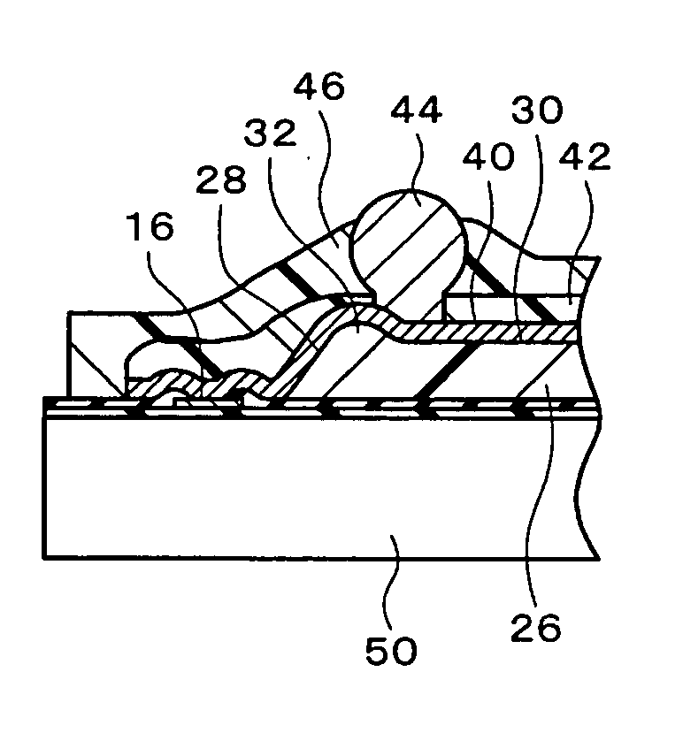
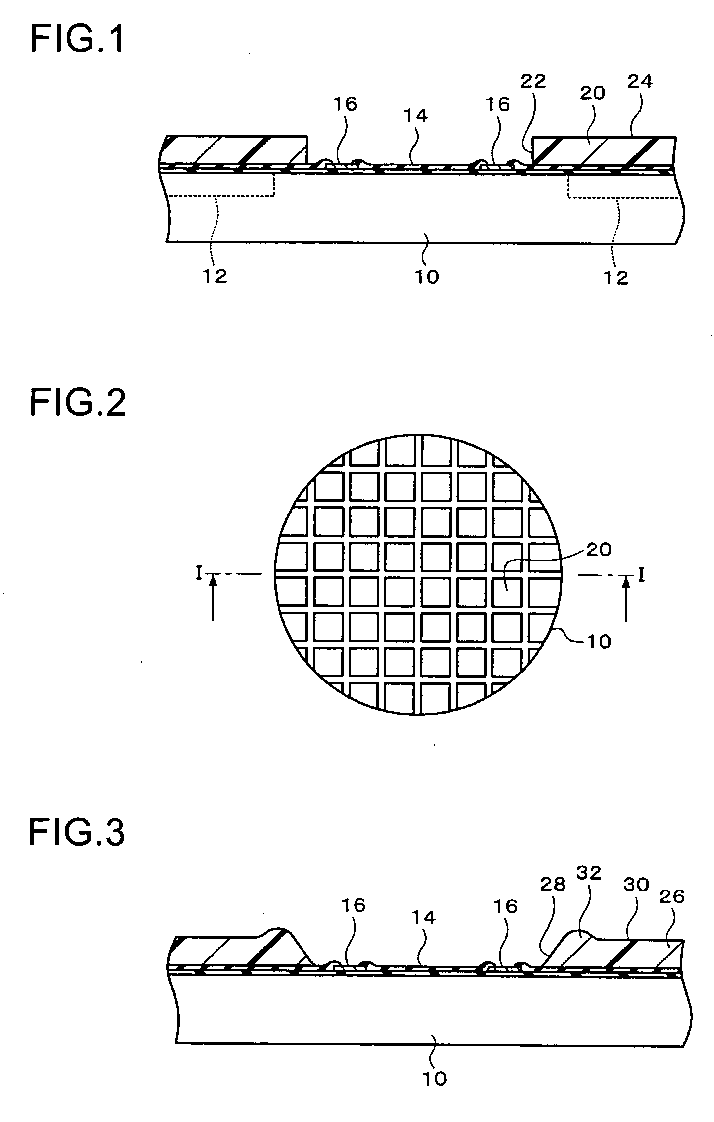
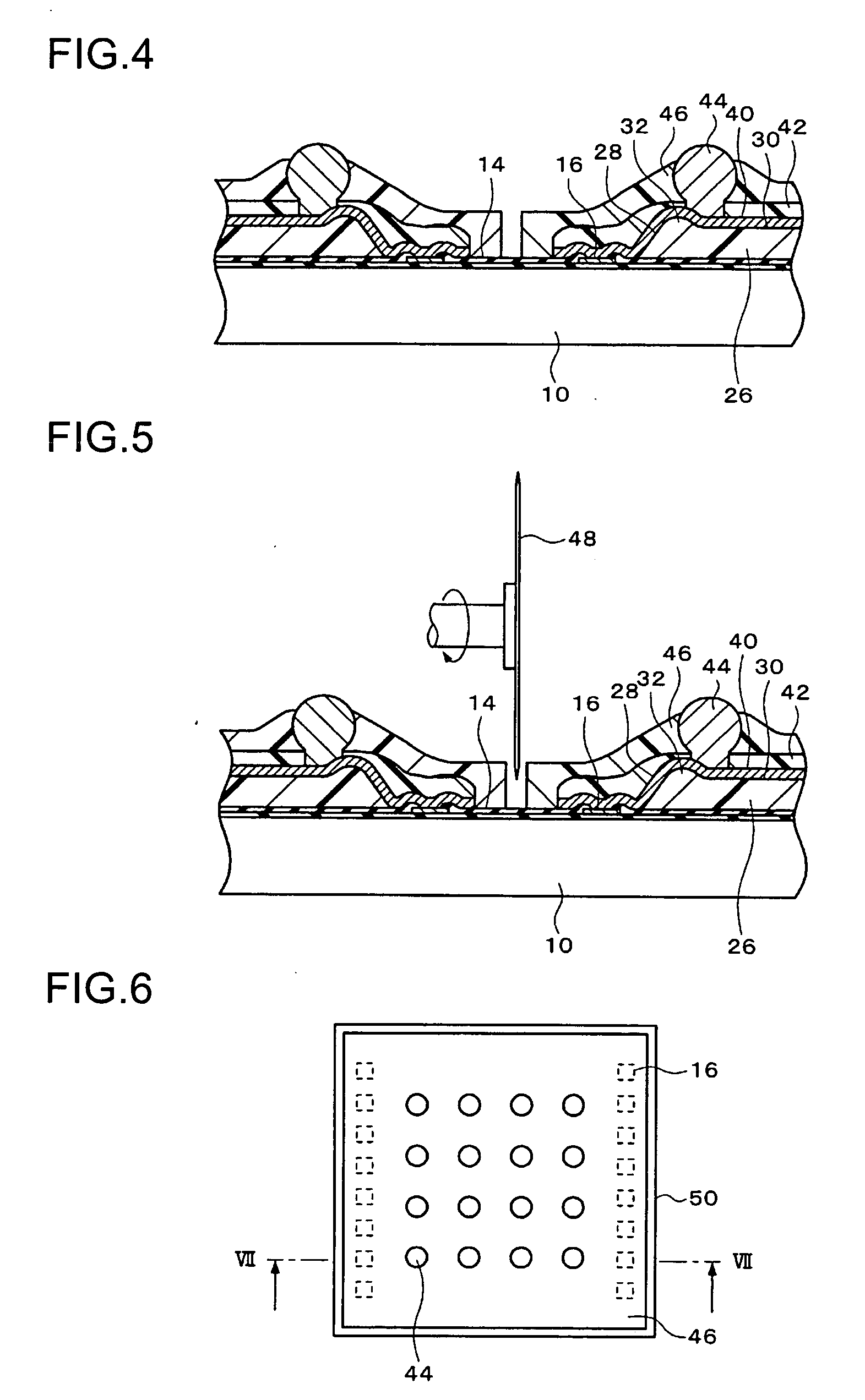
[0026] FIGS. 1 to 5 illustrate a method for manufacturing the semiconductor device according to the present invention. In this embodiment, a semiconductor substrate 10 is used. The semiconductor substrate 10 includes a plurality of integrated circuits 12. When the semiconductor substrate 10 is cut into a plurality of separate semiconductor chips, the separated semiconductor chips have the respective integrated circuits 12.

[0027] A passivation layer 14 may be formed on a surface of the semiconductor substrate 10. For example, the passivation layer 14 may be formed of an inorganic material such as silicon dioxide (SiO2) or silicon nitride (SiN). The passivation layer 14 may include a plurality of sublayers. In this case, at least one sublayer (for example, the uppermost sublayer) may be formed of an organic material.

[0028] The bonding pads 16 are formed on the semiconductor substrat...


PUM


Abstract

A semiconductor wafer includes a semiconductor substrate having a plurality of integrated circuits and electrical interconnections electrically connected to each of the integrated circuits. The semiconductor substrate includes bonding pads formed on a surface of the semiconductor substrate. Each of the bonding pads is part of a corresponding electrical interconnection. First resin layers are each disposed on each of a plurality of areas on the semiconductor substrate and have ridged edges. Wirings are each disposed over a corresponding bonding pad and a corresponding first resin layer and are electrically connected to the corresponding bonding pad. External connection terminals are each disposed on a corresponding wiring and are electrically connected to the corresponding wiring.

Description

BACKGROUND OF THE INVENTION [0001] 1. Field of the Invention [0002] The present invention relates to a semiconductor wafer, a semiconductor device, a method for manufacturing the semiconductor device, a circuit board, and an electronic apparatus. [0003] 2. Description of the Related Art [0004] Bare chip mounting is preferable for high density mounting in semiconductor devices. However, quality control and handling of bare chips are difficult. For this reason, a semiconductor device to which the chip size / scale package (CSP) technology is applied has been developed. Particularly, in recent years, the wafer level CSP has received attention. In the wafer level CSP, wirings are formed on a first resin layer, the entire wafer is packaged, and then the wafer is cut into separated packages. In the CSP, the external connection terminals (for example, solder balls) and wirings can be formed on only restricted areas. [0005] Accordingly, an advantage of the present invention is to provide incr...

Claims


Application Information

Patent Timeline
Patent Type & Authority Applications(United States)
IPC IPC(8): H01L23/52H01L21/3205H01L23/12H01L23/31
CPCH01L23/3114H01L23/3192H01L2924/3025H01L2924/0002H01L2924/00H01L24/02H01L24/03H01L24/05H01L24/11H01L24/13H01L24/16H01L2224/0231H01L2224/0236H01L2224/02377H01L2224/05001H01L2224/05022H01L2224/05147H01L2224/05166H01L2224/05184H01L2224/05548H01L2224/05647H01L2224/05666H01L2224/05684H01L2224/06131H01L2224/10126H01L2224/13022H01L2224/13024H01L2924/0001H01L2924/00014H01L2224/02
Inventor OBINATA, TAKAYOSHI
Owner SEIKO EPSON CORP
Why Eureka
Try Eureka