

Semiconductor device and a method of manufacturing the same
- Summary
- Abstract
- Description
- Claims
- Application Information
AI Technical Summary
Benefits of technology
Problems solved by technology
Method used
Image

Examples
first embodiment
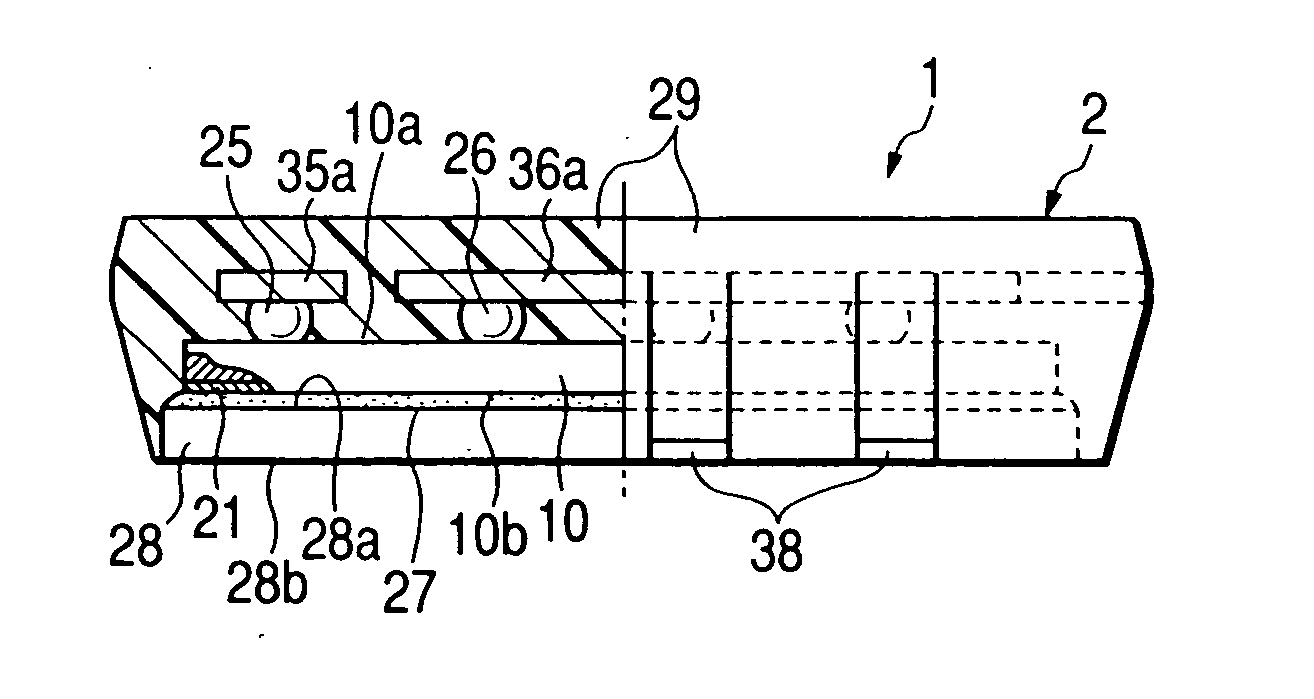
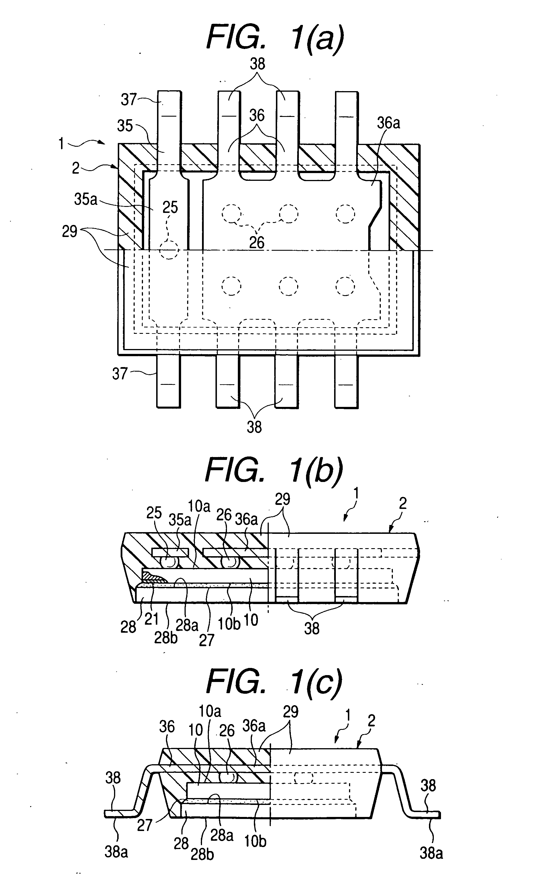
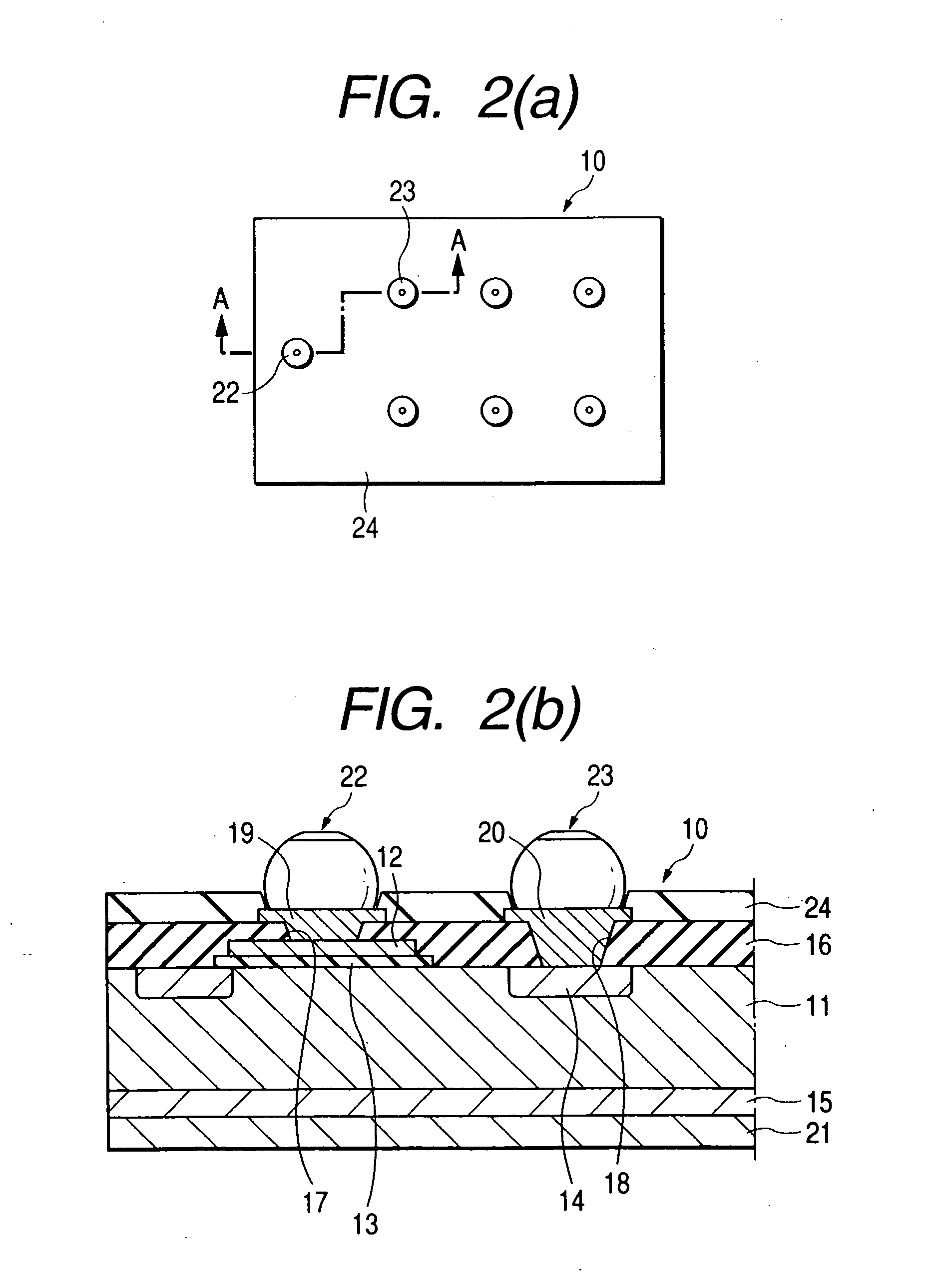
the invention will now be described with reference to an illustration of a structure of a MOSFET in FIGS. 1A, 1B and 1C and illustrations of a method of manufacturing the MOSFET shown in FIGS. 2A though 8B.
A semiconductor device according to the first embodiment is a field effect transistor referred to as “MOSFET (metal oxide semiconductor field effect transistor)”, and a MOSFET 1 is a power MOS transistor that generates high output and high heat.
Referring to a schematic configuration of the MOSFET 1 shown in FIGS. 1(a) through 1(c), it comprises a semiconductor pellet 10 having a field effect transistor fabricated on a principal surface 10a thereof and formed in a compact plate-like configuration, a plurality of inner leads 35 and 36 for electrically conducting the field effect transistor element to the outside, a gate connecting piece 35a (inner lead coupling portion) for supporting two inner leads 35, a gate connecting portion (connecting portion) 25 constituted by a protrudin...
second embodiment
the invention will now be described with reference to illustrations in FIGS. 9(a) through 12 showing a structure of a MOSFET, illustrations in FIGS. 13 through 22(b) showing a method of manufacturing a MOSFET, illustrations in FIGS. 23(a) through 25 showing effects of a MOSFET and illustrations in FIGS. 27(a) and 27(b) showing a header frame of a MOSFET as a comparative example and the mounting of the header frame.
In the plan views of FIGS. 11(a), 12, 23(a), 23(b) and 24(a), like members are indicated by like hatching.
A MOSFET 70 which is a semiconductor device according to a second embodiment of the invention is a power MOS transistor that generates high output and high heat similar to the MOSFET 1 in the first embodiment.
In the MOSFET 70, as shown in FIG. 9(b), three source outer leads 38 and one gate outer lead 37 bent in a gull wing configuration protrude from one of two opposite lateral surfaces of a resin encapsulant 29 and, as shown in FIG. 9(a), a plate-like and substan...
PUM
 Abstract
Description
Claims
Application Information