Semiconductor device with strain relieving bump design

a technology of semiconductor components and bumps, applied in semiconductor devices, solid-state devices, basic electric elements, etc., can solve problems such as mechanical and/or electrical failure of joints, electrical failures, and increase the complexity and manufacturing cost of devices

Inactive Publication Date: 2005-02-03
MOTOROLA INC +1
View PDF4 Cites 22 Cited by
  • Summary
  • Abstract
  • Description
  • Claims
  • Application Information

AI Technical Summary

Benefits of technology

[0010] In one aspect, a device is provided which comprises (a) a semiconductor die or other substrate having a contact pad thereon, (b) a redistribution conductor having a base portion which is in electrical communication with the contact pad, and having a convoluted, laterally extending portion, and (c) a (typically organic) passivation layer disposed between the laterally extending portion and the die, and wherein the laterally extending portion preferably forms a frangible bond to the passivation layer. The device may also comprise a bumped contact in electrical communication with the redistribution conductor. The laterally extending portion may be serpentine or shaped like a sine wave, and preferably changes direction at least once, more preferably at least twice, and most preferably at least three times in going from the base to the bumped contact. The laterally extending portion has an average minimum thickness of at least about 3 microns, preferably within the range of about 8 to about 16 microns, and more preferably within the range of about 10 to about 14 microns, as measured along an axis extending through the center of, and orthogonal to, the laterally extending portion. The device may further comprise a PCB substrate in contact with said bumped contact, in which case the PCB substrate is preferably separated from the redistribution conductor by an open space rather than an underfill. The device preferably also comprises a dewetting agent disposed on surfaces of the laterally extending portion of the redistribution conductor. This dewetting agent, which is preferably sufficiently conductive so as to permit probing of the conductor and is typically about 200 nm in thickness, serves to prevent solder from wetting the redistribution conductor beyond the bump contact region, hence confining the solder bump to an area directly above the bump pad. The dewetting agent can be, but is not limited to, one or more of the materials (e.g., TiW) used as a seed metal for electroplating the redistribution conductor metal.

Problems solved by technology

Over time, these stresses can result in mechanical and / or electrical failure of the joint.
Indeed, in devices of this type, the redistribution conductors are typically too thin to withstand any significant amount of stress by themselves and tend to break if exposed to significant stresses, thus resulting in electrical failures.
For example, the addition of a third passivation layer increases the complexity and manufacturing cost of the device, while also making it more difficult to rework the device or to perform electrical probing on the redistribution conductor.

Method used


Image

  • Semiconductor device with strain relieving bump design
  • Semiconductor device with strain relieving bump design
  • Semiconductor device with strain relieving bump design

Examples


Embodiment Construction

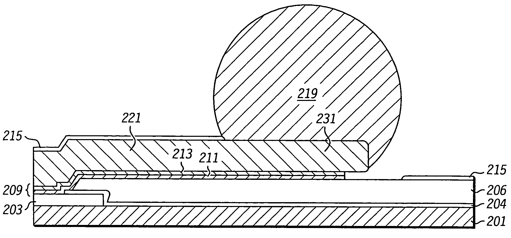
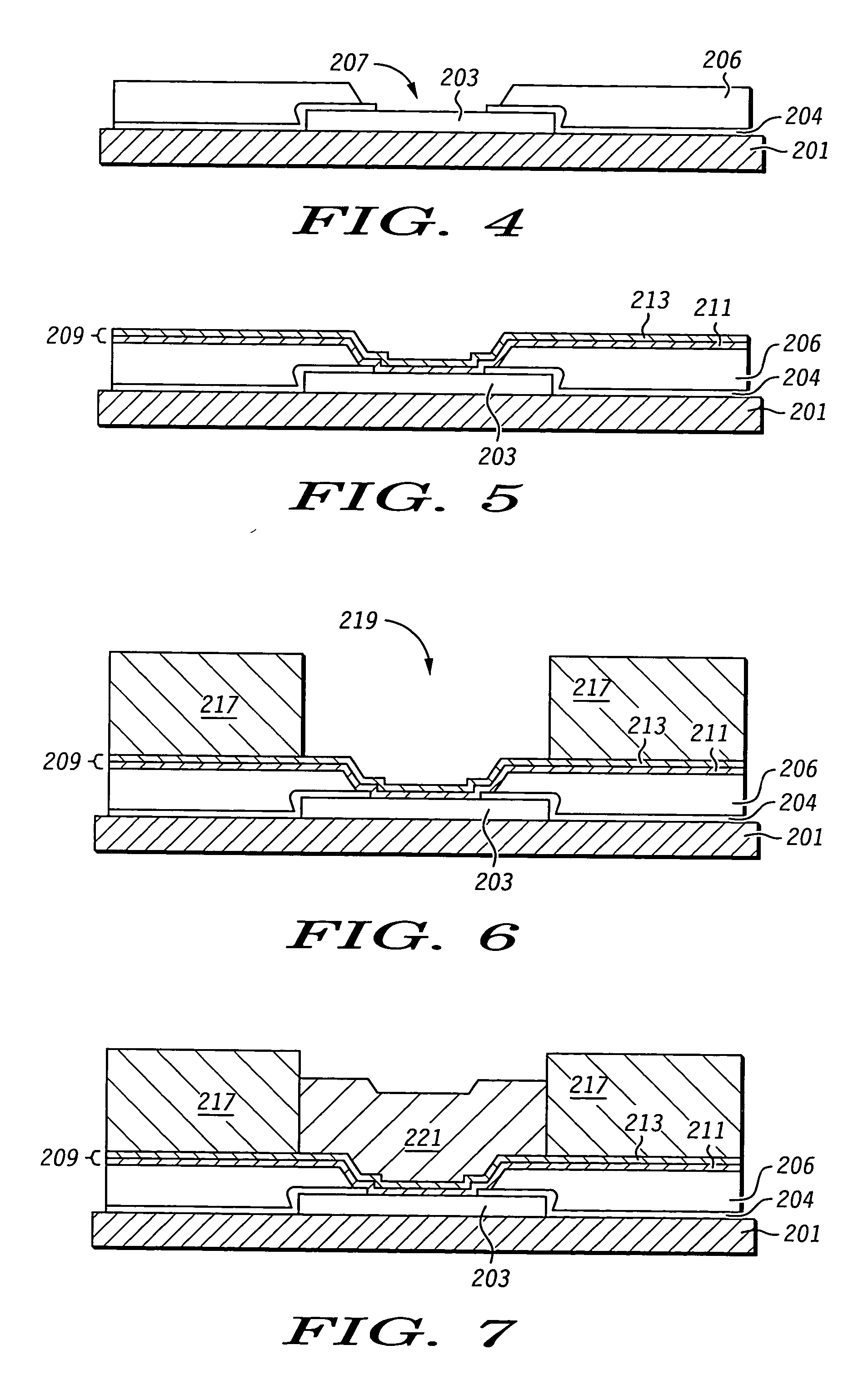
[0022] It has now been found that the above noted needs may be met by providing bumped semiconductor devices with redistribution conductors that are capable of releasing or delaminating from an underlying passivation layer and flexing so as to alleviate CTE differential stress, and which are thick enough so as to be able to withstand such flexing without electrical failure. Such redistribution conductors are described in greater detail below.

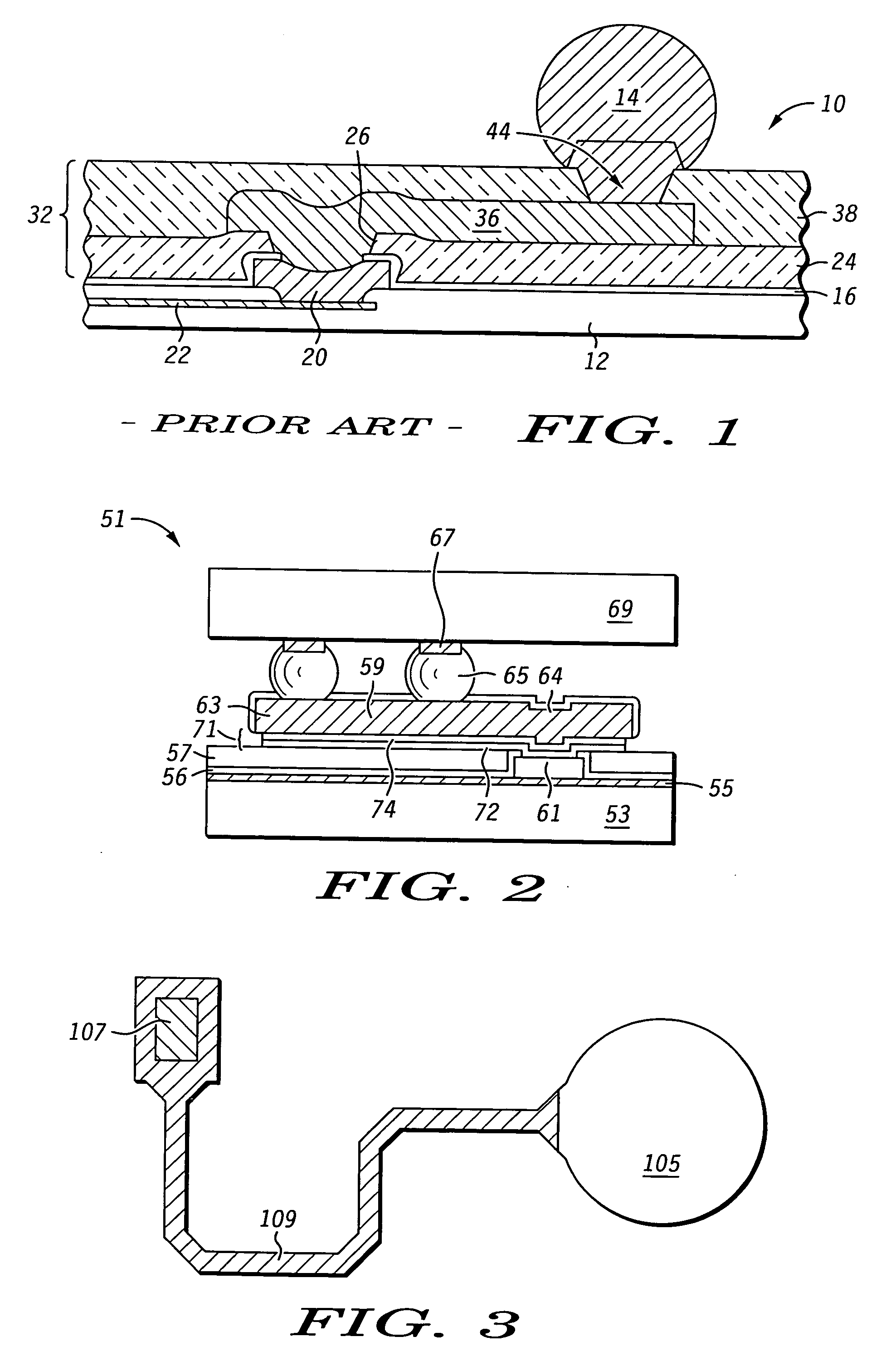
[0023]FIG. 2 illustrates one example of a bumped semiconductor device 51 made in accordance with the teachings herein. For convenience of illustration, the device features and dimensions have been exaggerated in some aspects and condensed into a single plane, and a redistribution conductor 59, which is preferably essentially serpentine in shape (see FIG. 3), is depicted simply as straight conductor to allow for understanding of the device in a 2-dimensional cross-sectional drawing. However, one skilled in the art will appreciate that, in an act...


PUM


Abstract

A semiconductor device (51) is provided. The device (51) comprises a die (53) having a contact pad (61) thereon, a redistribution conductor (59) having a base portion (64) which is in electrical communication with the contact pad (61) and a laterally extending portion (63), a bumped contact (65) which is in electrical communication with the redistribution conductor (59), and a passivation layer (57) disposed between the laterally extending portion (63) of the redistribution conductor (59) and the die (53). Preferably, the redistribution conductor (59) is convoluted and is adapted to peel or delaminate from the passivation layer (57) under sufficient stress so that it can shift relative to the passivation layer (57) and base portion (64) to relieve mechanical stress between substrate (69) and the die (53). Bump and coiled redistribution conductor (59) accommodating small CTE mis-match strain without failure allows DCA flip-chip to be reliable without underfill or additional assembly process.

Description

FIELD OF THE INVENTION [0001] The present invention relates generally to bumped semiconductor components, and more particularly to bumped semiconductor components equipped with redistribution circuitry and suitable for wafer level BGA packaging. BACKGROUND OF THE INVENTION [0002] Semiconductor components such as die, chip scale packages, ball grid arrays (BGAs), and wafers frequently include terminal contacts in the form of metal bumps. Components equipped with such contacts are often referred to as “bumped” components. [0003]FIG. 1 illustrates one type of prior art flip chip semiconductor package. The package 10 comprises a semiconductor die 12 and an array of bumped contacts 14 on the circuit side of the die 12. The bumped contacts 14 allow the package 10 to be surface mounted to a substrate, such as a printed circuit board (PCB). Typically, the bumped contacts 14 are made of solder, which allows the package 10 to be bonded to a substrate using a solder reflow process. [0004] The ...

Claims


Application Information

Patent Timeline
Patent Type & Authority Applications(United States)
IPC IPC(8): H01L21/60H01L23/31H01L23/485
CPCH01L23/3114H01L2224/0401H01L2224/0231H01L2224/1147H01L2224/13099H01L2924/01005H01L2924/01013H01L2924/01015H01L2924/01022H01L2924/01029H01L2924/01033H01L2924/01039H01L2924/01057H01L2924/01074H01L2924/01078H01L2924/01082H01L2924/01322H01L2924/14H01L2924/01006H01L2924/014H01L2224/02335H01L24/11H01L24/03H01L24/05H01L24/08H01L24/13H01L24/16H01L2224/13027H01L2224/081H01L2224/05569H01L2224/05008H01L2224/05548H01L2224/0235H01L2924/00012H01L23/48
Inventor WANG, JAMES JEN-HOJANG, JIN-WOOKMENDOZA, ALFREDORUNTON, RAJASHISHUMWAY, RUSSELL
Owner MOTOROLA INC
Why Eureka
Try Eureka