Semiconductor apparatus including a radiator for diffusing the heat generated therein

a technology of electromagnetic radiation and electromagnetic shielding layer, which is applied in the direction of electrical apparatus, semiconductor devices, and semiconductor/solid-state device details, which can solve the problems of insufficient protection of the wiring layer in the esd protection circuit, the inability to reduce the temperature of the metal wiring layer according to conventional techniques, and the likely breakage of the eds protection elemen

Active Publication Date: 2005-02-03
KK TOSHIBA
View PDF3 Cites 53 Cited by
  • Summary
  • Abstract
  • Description
  • Claims
  • Application Information

AI Technical Summary

Problems solved by technology

Eventually, when too much voltage input is supplied to the internal circuit, a breakdown of the EDS protection element will likely occur at the level of individual elements in the EDS protection element, such as at a gate element or a resistance element in a metal-oxide semiconductor field-effect transistor (MOSFET).
However, this measure is insufficient for protecting the wiring layer in the ESD protection circuit, since excessive current flow due to the excessive voltage input into the ESD protection circuit easily exceeds over many tens to hundreds times of a permitted current density (defined by electromigration (ED)) in the wiring layer acting as a surge current path.
Consequently, the generated heat that is caused by such a large surge current may easily fuse the wiring layers for connecting to the internal circuit.
Accordingly, the temperature increase of the metal wiring layer cannot be reduced according to conventional techniques.
However, this proposal is also insufficient for protecting a wiring layer as a surge current path from an excessive voltage input into the ESD protection circuit.

Method used


Image

  • Semiconductor apparatus including a radiator for diffusing the heat generated therein
  • Semiconductor apparatus including a radiator for diffusing the heat generated therein
  • Semiconductor apparatus including a radiator for diffusing the heat generated therein

Examples


Embodiment Construction

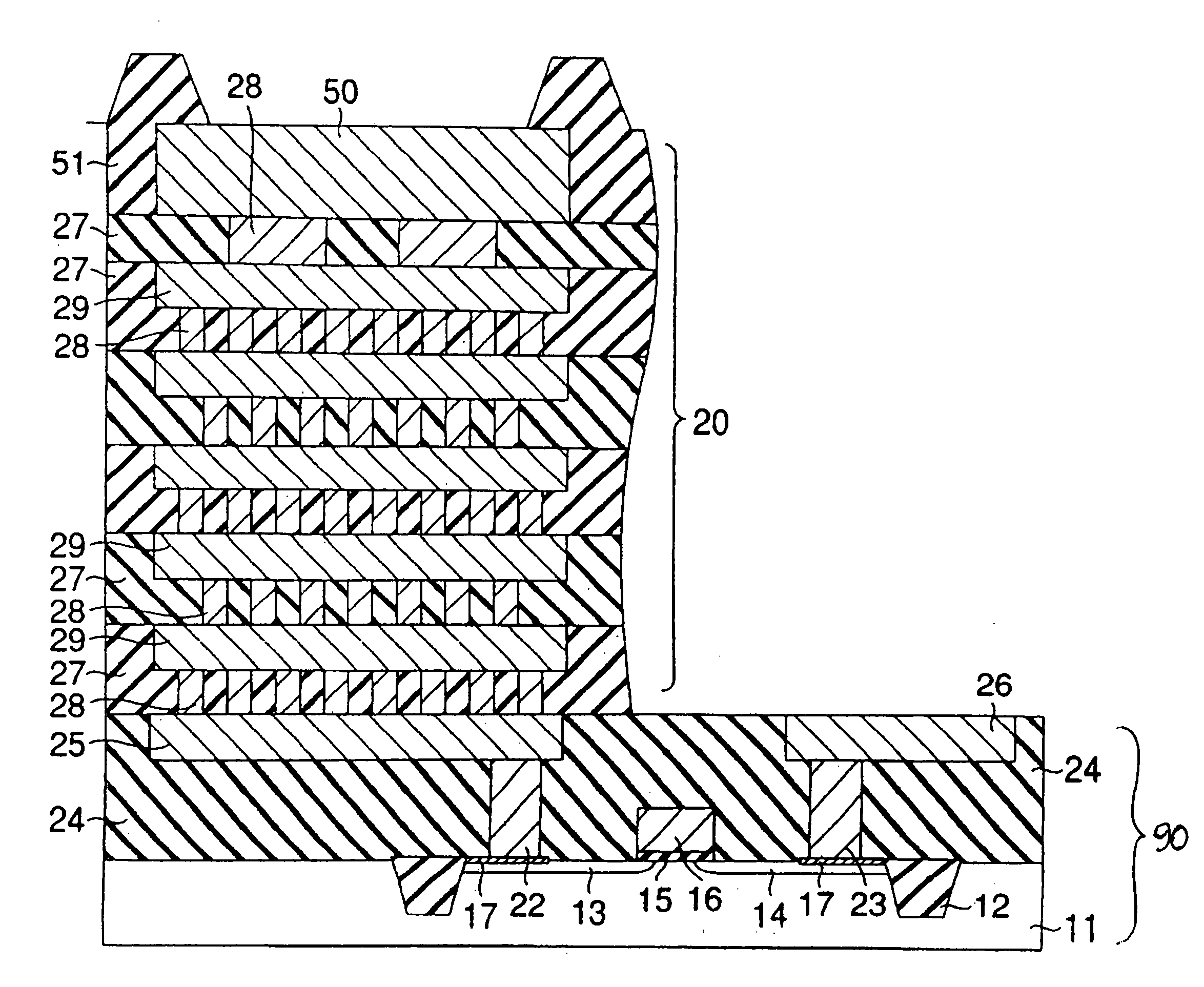
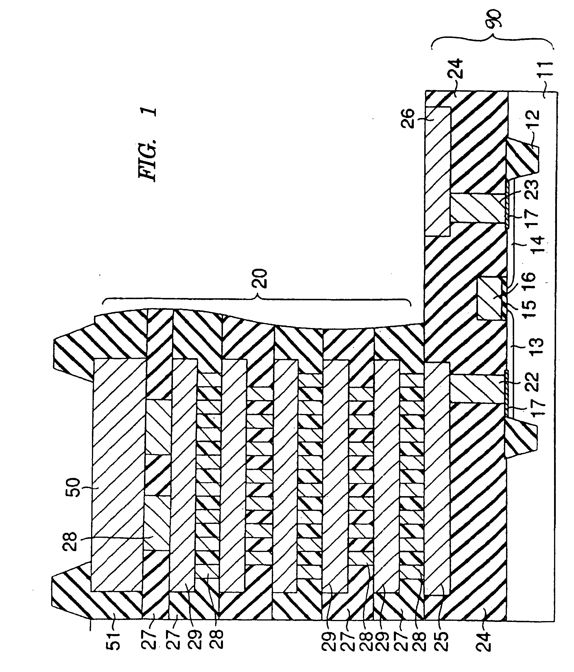
[0033] Reference will now be made in detail to the exemplary embodiments consistent with the present invention, examples of which are illustrated in the accompanying drawings. FIG. 1 illustrates an exemplary protection element used in an ESD protection circuit, and an exemplary radiator configuration coupled to a wiring in the ESD protection circuit. According to this embodiment, a protection element that is comprised of metal layers and alloy films is coupled to a wiring layer used as a surge current path of an ESD protection circuit for a semiconductor apparatus.

[0034] In an embodiment consistent with the present invention, a NMOSFET is used as a protection element for an ESD protection circuit by directly connecting a gate and a source of a NMOSFET, so as to construct a diode. One end of a protection element is connected to an input wiring that couples an input terminal (bonding pad) to an input terminal. The other end of the protection element is coupled to a grounding node.

[0...


PUM


Abstract

A semiconductor apparatus is provided that includes a radiator for efficiently radiating heat generated in a wiring layer used in a surge current path of an electrostatic discharge protection circuit, and also for protecting the wiring layer itself used as the surge current path. The semiconductor apparatus includes an input protection circuit coupled to a wiring provided between an external terminal and an internal circuit, the input protection circuit includes a protection element for protecting the internal circuit from an excessive electrostatic surge input supplied to the external terminal. The semiconductor apparatus further includes a first metal wiring layer coupled to the input protection circuit and included in a current path for the surge electrostatic surge input, and a radiator including a sufficient thermal conductivity material coupled to the first metal wiring layer.

Description

CROSS-REFERENCE TO RELATED APPLICATIONS [0001] This application claims priority from, and the benefit of, Japanese Application No. 2003-178237, filed on Jun. 23, 2003, the contents of which are expressly incorporated herein by reference in their entirety. BACKGROUND OF THE INVENTION [0002] 1. Field of the Invention [0003] The present invention relates to a semiconductor apparatus, including an electrostatic discharge protection circuit (hereinafter referred to as an “ESD protection circuit”) for protecting internal circuits from electrostatic discharge (hereinafter simply referred to as “ESD”) caused by too much electrostatic input through an external circuit, and more particularly, to a semiconductor apparatus including a radiator for diffusing the heat generated in the ESD protection circuit. [0004] 2. Description of the Background Art [0005] To understand an example of an ESD protection circuit for a semiconductor apparatus, an equivalent circuit of an ESD protection circuit is i...

Claims


Application Information

Patent Timeline
Patent Type & Authority Applications(United States)
IPC IPC(8): H01L21/3205H01L23/52H01L21/822H01L23/367H01L23/485H01L27/04H01L29/417
CPCH01L23/367H01L23/3677H01L2924/1306H01L2224/05556H01L2224/02166H01L2924/01055H01L2924/01033H01L24/05H01L29/41725H01L2224/05093H01L2224/05624H01L2224/05647H01L2924/01004H01L2924/01006H01L2924/01013H01L2924/01014H01L2924/01015H01L2924/01022H01L2924/01029H01L2924/0105H01L2924/01074H01L2924/04953H01L2924/13091H01L2924/00014H01L2924/00
Inventor MATSUNAGA, TAKASHIUSUI, TAKAMASA
Owner KK TOSHIBA
Why Eureka
Try Eureka