Phase interpolator circuitry for reducing clock skew

Inactive Publication Date: 2005-02-03
NEC ELECTRONICS CORP
View PDF12 Cites 66 Cited by
  • Summary
  • Abstract
  • Description
  • Claims
  • Application Information

AI Technical Summary

Benefits of technology

Specifically, one object of the present invention is to provide a phase interpolation circuitry for achieving stabilized interpolation of multiphase clocks with reduced clo

Problems solved by technology

In a data transfer system adopting clock and data recovery, a receiver reproduces a synchronized clock signal from a data signal received from a transmitter using a clock generator, typically including a quartz oscillator and a frequency multiplier, such as a PLL (phase lock loop) circuit; the transmitter does not provide the receiver with any clock signal for achieving synchronization.
A clock and data recovery technique requires generating a high-frequency clock within a receiver for achieving high-speed data transmission; however, a receiver often experiences a difficulty in generatin

Method used


Image

  • Phase interpolator circuitry for reducing clock skew
  • Phase interpolator circuitry for reducing clock skew
  • Phase interpolator circuitry for reducing clock skew

Examples


first embodiment

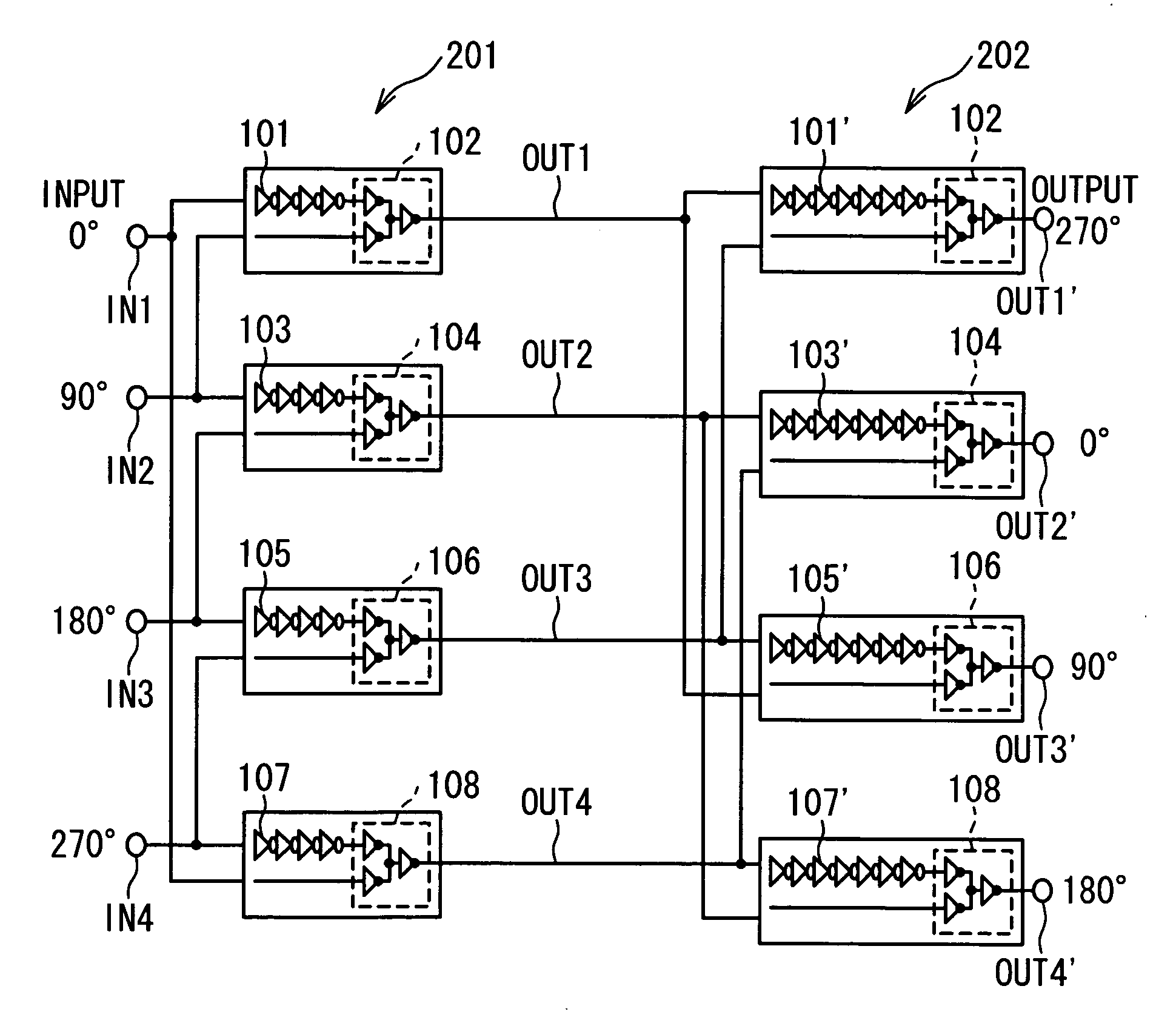
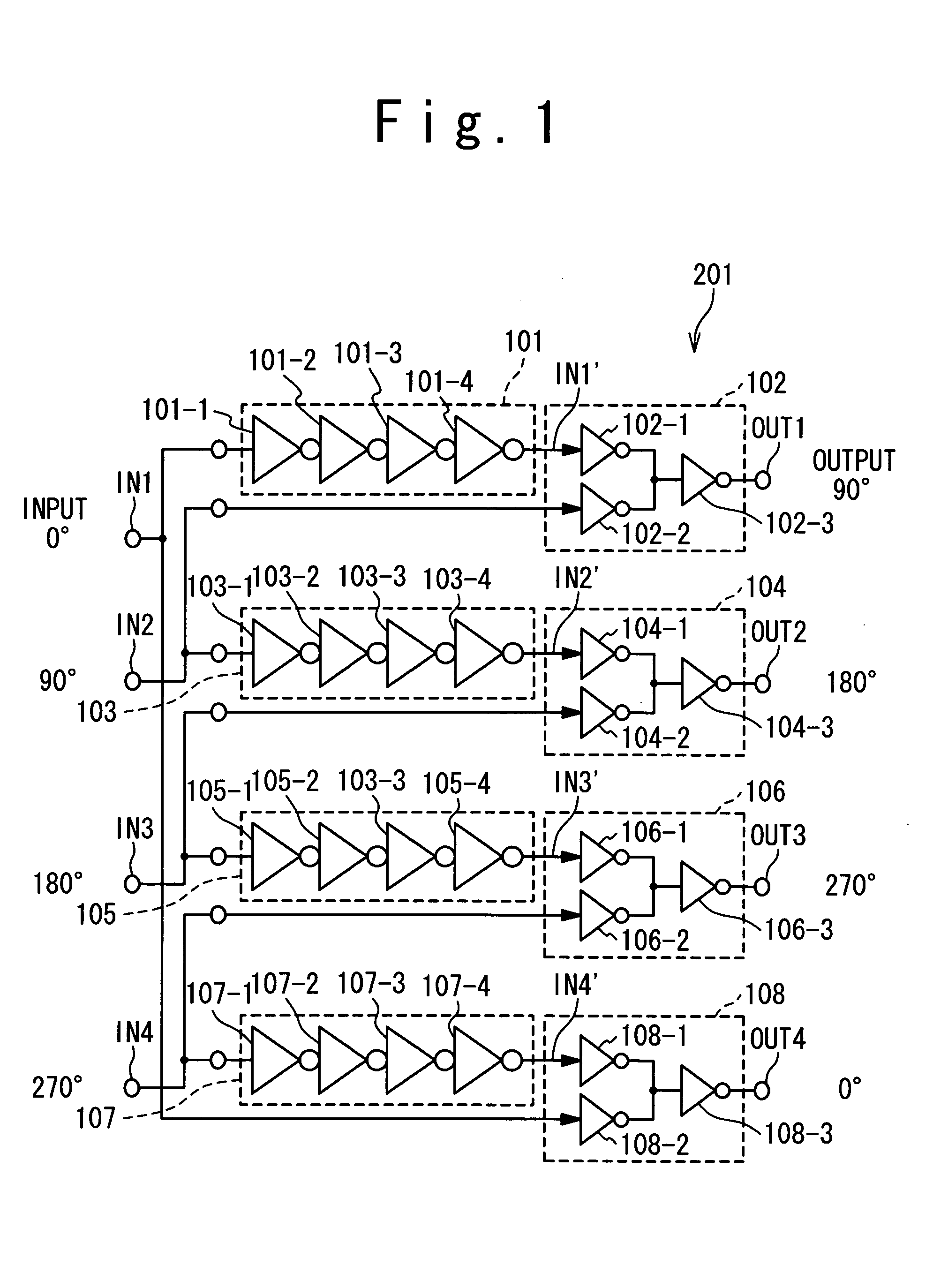
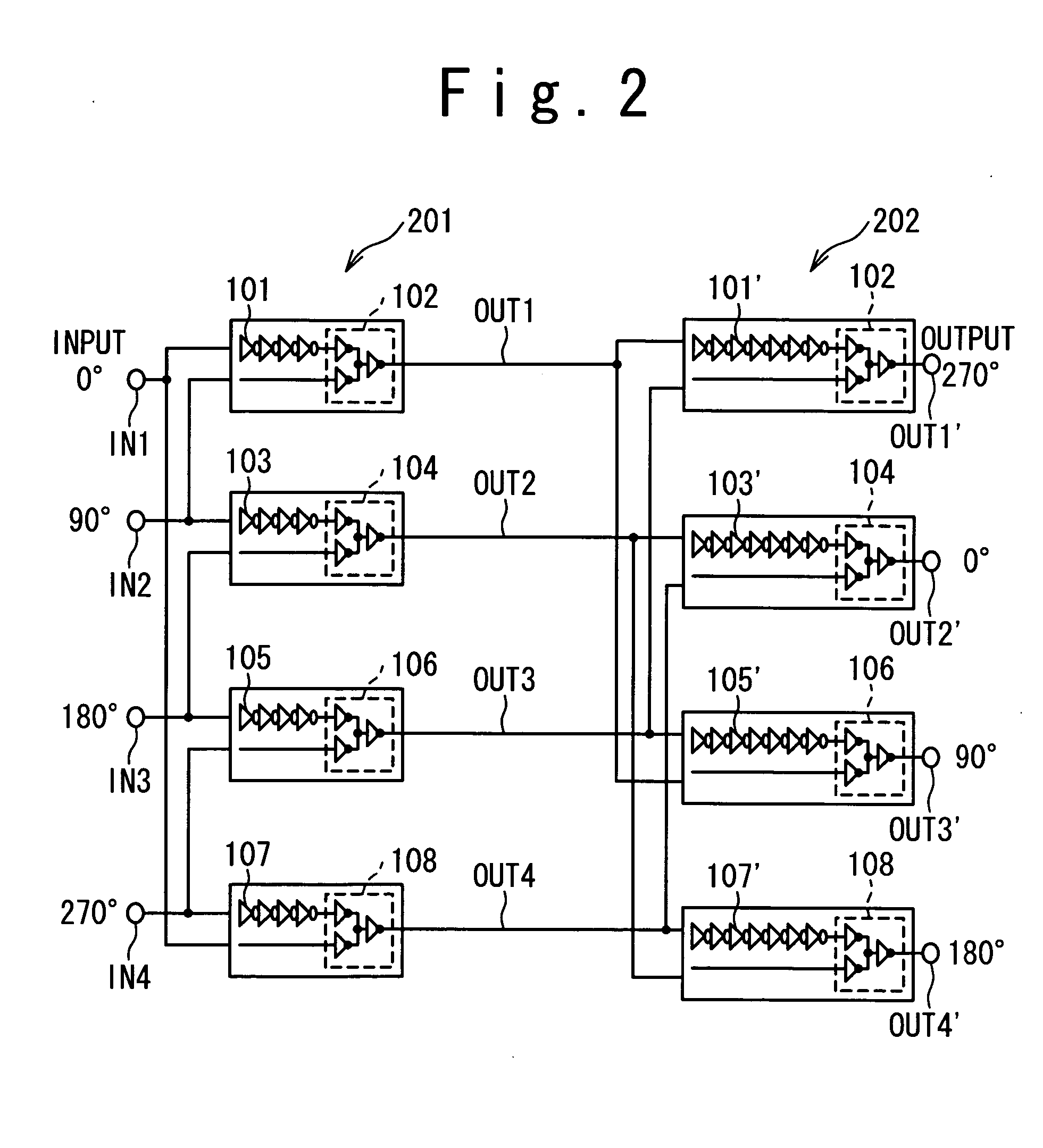
In a first embodiment, as shown in FIG. 3, a phase interpolation circuitry for multiphase clocks is composed of four delay lines 2, 4, 6, and 8, and four phase blender circuits 1, 3, 5, and 7. The delay lines 2, 4, 6, and 8 are composed of series-connected inverters. In FIG. 3, the inverters within the delay line 2 are denoted by numerals 2a through 2d, the inverters within the delay line 4 are denoted by numerals 4a through 4d, the inverters within the delay line 6 are denoted by numerals 6a through 6d, and the inverters within the delay line 8 are denoted by numerals 8a through 8d.

The delay lines 2, 4, 6, and 8 receives input clock signals IN1, IN2, IN3, and IN4, which are equally phased at constant intervals of 90° in an ideal state; the ideal phases of the input clock signals IN1, IN2, IN3, and IN4 are defined as being 0°, 90, 180°, and 270°, respectively. The delay lines 2, 4, 6, and 8 provide a delay of 90° for the input clock signals IN1, IN2, IN3, and IN4. The delayed clo...

second embodiment

In a second embodiment, as shown in FIG. 8, constant current sources, denoted by numerals 21 to 28, 41 to 48, 61 to 68, and 81 to 88, are additionally connected to the power and ground terminals of the serial-connected inverters within the delay lines 2, 4, 6, and 8. The constant current sources 21 to 28, 41 to 48, 61 to 68, and 81 to 88 effectively regulates the pull-up and pull-down currents, that is, the rise / fall times of the serial-connected inverters within the delay lines 2, 4, 6, and 8, and thereby stabilize the delay times of the delay lines 2, 4, 6, and 8 against the undesirable manufacture variance and the changes in the operation temperature and the power supply voltage. This effectively reduces the clock skews between the output clock signals OUT1 to OUT4.

In an alternative embodiment, as shown in FIG. 9, the constant current sources between the serial-connected inverters and ground, denoted by the numerals 22, 24, 26, 28, 42, 44, 46, 48, 62, 64, 66, 68, 82, 84, 86, a...

third embodiment

In a third embodiment, as shown in FIG. 11, each of the phase blender circuits 1, 3, 5, 7 additionally include a pair of constant current sources, one disposed between the power terminal of the output inverter and the power supply, and the other between the ground terminal and ground; the constant current sources connected to the power terminals of the output inverters are denoted by numerals 15, 35, 55, and 75, and the constant current sources connected to the ground terminals are denoted by numerals 16, 36, 56, and 76.

The additional constant current sources 15, 16, 35, 36, 55, 56, 75, and 76 effectively regulate the pull-up and pull-down currents, that is, the rise / fall times of the output inverters 1c, 3c, 5c, and 7c within the phase blender circuit 1, 3, 5, and 7, and thereby stabilize the delay times of the phase blender circuit 1, 3, 5, and 7 against the undesirable manufacture variance and the changes in the operation temperature and the power supply voltage. This effectiv...


PUM


Abstract

A phase interpolator circuitry is composed of a delay line, and a phase blender circuit. The delay line delays a first input clock signal to develop a delayed clock signal. The phase blender circuit includes a first inverter receiving the delayed clock signal, and a second inverter receiving a second input clock signal phased away from the first input clock signal. The outputs of the first and second inverters are commonly coupled together. The phase interpolator circuitry additionally includes at least one of constant current sources: first one connected between a power terminal of the first inverter and a power supply, second one connected between a ground terminal of the first inverter and ground, third one connected between a power terminal of the second inverter and a power supply, and fourth one connected between a ground terminal of the second inverter and ground.

Description

BACKGROUND OF THE INVENTION 1. Field of the Invention The present invention is generally related to phase interpolator circuitries, more particularly, to skew reduction in phase interpolator circuitries suitable for multiphase clocks. 2. Description of the Related Art Clock and data recovery is one of the widely known techniques used for high-speed data transmission. In a data transfer system adopting clock and data recovery, a receiver reproduces a synchronized clock signal from a data signal received from a transmitter using a clock generator, typically including a quartz oscillator and a frequency multiplier, such as a PLL (phase lock loop) circuit; the transmitter does not provide the receiver with any clock signal for achieving synchronization. A clock and data recovery technique eliminates a need for transmitting a high-frequency clock signal between a transmitter and a receiver, and thereby facilitates high-speed data transmission. A clock and data recovery technique req...

Claims


Application Information

Patent Timeline
IPC IPC(8): G06F1/04G06F1/06H03K5/00H03K5/13H03K5/15H03K17/693H04L25/14
CPCH03K5/133H03K17/693H04L25/14H03K2005/00202H04L7/0025H03K2005/00039
Inventor KUBO, SATORUOTAKE, TOSHIKAZU
Owner NEC ELECTRONICS CORP
Why Eureka
Try Eureka