Supercharge Your Innovation With Domain-Expert AI Agents!

Method for producing and testing a corrosion-resistant channel in a silicon device

a technology of corrosion resistance and silicon, which is applied in the direction of semiconductor/solid-state device testing/measurement, semiconductor/solid-state device details, instruments, etc., can solve the problems of gas passingivating the material and corroding any exposed silicon

Inactive Publication Date: 2005-02-03
SMC CORP
View PDF7 Cites 0 Cited by
  • Summary
  • Abstract
  • Description
  • Claims
  • Application Information

AI Technical Summary

Benefits of technology

This method provides reliable and complete protection against fluorine and other corrosive fluids, ensuring the integrity of MEMS devices by identifying and preventing corrosion, while using less toxic and corrosive compounds, and effectively bonding multilayer devices without damaging them.

Problems solved by technology

The gas will passivate the material and corrode any exposed silicon.

Method used


Image

  • Method for producing and testing a corrosion-resistant channel in a silicon device
  • Method for producing and testing a corrosion-resistant channel in a silicon device
  • Method for producing and testing a corrosion-resistant channel in a silicon device

Examples


Embodiment Construction

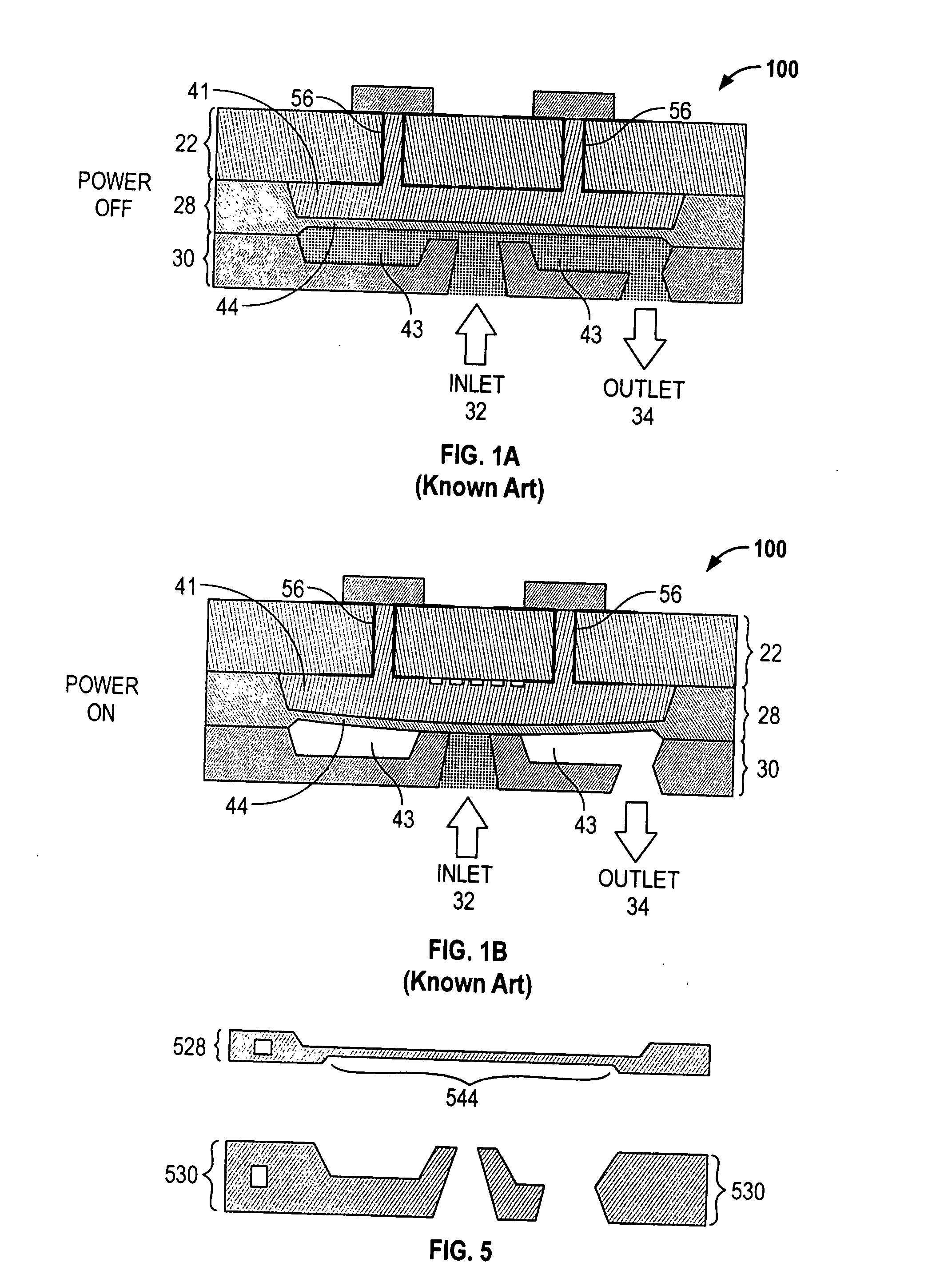
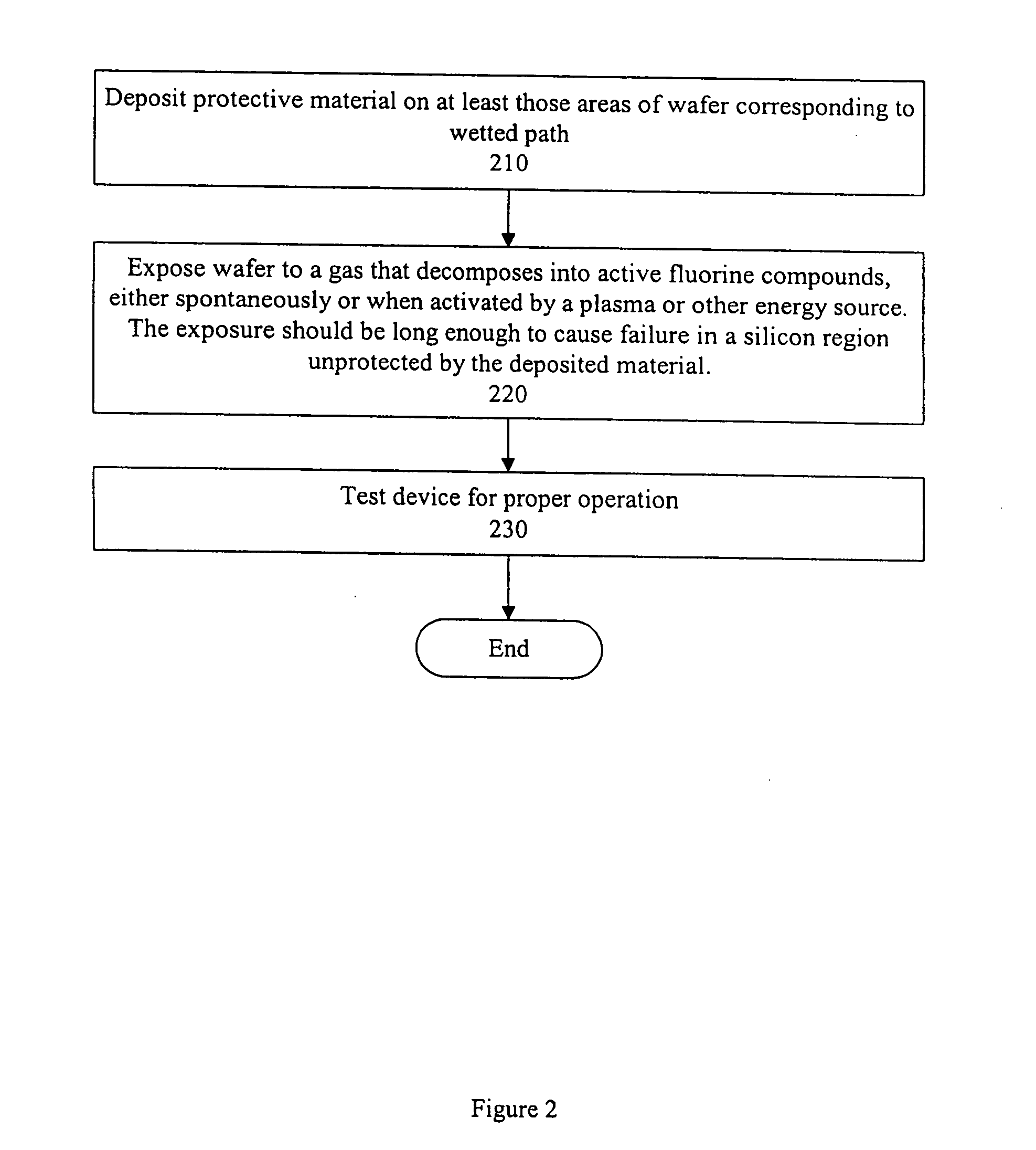
[0031]FIG. 2 illustrates a method for producing and testing a corrosion-resistant wetted path in a silicon device according to one embodiment of the present invention. Starting with a silicon wafer(s) in which the wetted path has been formed, the protective material is applied 210 to at least those portions of the silicon wafer(s) corresponding to the wetted path. As described in further detail below, examples of such protective material include (1) a metal, such as aluminum or nickel, that can be passivated by fluorine compounds or (2) an organic compound, such as BCB, that is either resistant to fluorine or can be passivated by fluorine.

[0032] The wafer (or multi-layer wafer structure if applicable) is then exposed 220 to a gas that decomposes into active fluorine compounds, either spontaneously or when activated by a plasma or other energy source. An advantage of using an unreactive gas that requires an energy source to decompose into fluorine compounds, such as CF4, is that the...


PUM


Abstract

A method for producing a corrosion-resistant channel in a wetted path of a silicon device enables such device to be used with corrosive compounds, such as fluorine. A wetted path of a MEMS device is coated with either (1) an organic compound resistant to attack by atomic fluorine or (2) a material capable of being passivated by atomic fluorine. The device is then exposed to a gas that decomposes into active fluorine compounds when activated by a plasma discharge. One example of such a gas is CF4, an inert gas that is easier and safer to work with than volatile gases like ClF3. The gas will passivate the material (if applicable) and corrode any exposed silicon. The device is tested in such a manner that any unacceptable corrosion of the wetted path will cause the device to fail. If the device operates properly, the wetted path is deemed to be resistant to corrosion by fluorine or other corrosive compounds, as applicable.

Description

BACKGROUND OF THE INVENTION [0001] 1. Field of the Invention [0002] This invention relates generally to silicon devices (including MEMS devices) and more specifically to a method for producing and testing a corrosion-resistant channel in a silicon device. [0003] 2. Description of the Background Art [0004] A relatively recent development in the semiconductor industry is to use microelectromechanical systems (MEMS) in semiconductor and pharmaceutical manufacturing processes. MEMS devices are typically silicon chips that include miniaturized mechanical components, such as actuators, mirrors, levers, diaphragms, or sensors. MEMS devices may also include electronic circuitry. [0005] When MEMS devices are employed in semiconductor and pharmaceutical manufacturing processes, they are exposed to the chemical and biochemical substances used in such processes. The part of the MEMS device exposed to fluids (i.e., gases or liquids) during operation is commonly referred to as the “wetted path.” ...

Claims


Application Information

Patent Timeline
Patent Type & Authority Applications(United States)
IPC IPC(8): B81B7/00B81C99/00F16K99/00H01L21/02H01L21/66H01L23/544
CPCB81B7/0012H01L22/34B81B2201/058B81C99/0045B81C2203/038F16K99/0001F16K99/0015F16K99/0034F16K99/0036F16K99/0059F16K2099/0074H01L21/02071H01L22/20H01L22/24B81B2201/054
Inventor HARRIS, JAMES M.PATEL, SAPNA
Owner SMC CORP
Features
  • R&D
  • Intellectual Property
  • Life Sciences
  • Materials
  • Tech Scout
  • Unparalleled Data Quality
  • Higher Quality Content
  • 60% Fewer Hallucinations
Learn More