Method and composite for decreasing charge leakage

a semiconductor memory and charge leakage technology, applied in the field of semiconductor memories, can solve the problems of insufficient compactness, difficult to prevent electron migration through the insulator, impractical solution, etc., and achieve the effects of reducing the flow of phosphine, and reducing the flow of ammonia

Inactive Publication Date: 2005-02-03
MICRON TECH INC
View PDF32 Cites 7 Cited by
  • Summary
  • Abstract
  • Description
  • Claims
  • Application Information

AI Technical Summary

Benefits of technology

[0009] The dielectric composite insulator of the present invention, by reducing the charge leakage from the floating gate to the control gate of a memory cell, provides for an improved non-volatile semiconductor memory cell. Reducing the charge leakage in a non-volatile semiconductor memory makes the memory a more viable long term information storage device.
[0011] In one embodiment of the present invention, a layer of undoped polysilicon, amorphous silicon, or amorphous polysilicon is located between the floating gate and the layer of silicon dioxide. In an alternate embodiment of the present invention, a layer of silicon rich nitride is deposited on the layer of silicon nitride and then oxidized to form the silicon dioxide layer. In still another embodiment of the present invention, a layer of undoped polysilicon, amorphous silicon, or amorphous polysilicon is located between the floating gate and the silicon dioxide, and a layer of silicon rich nitride is located between the layer of silicon nitride and the silicon dioxide of the composite. The effect of interposing a layer of undoped polysilicon, amorphous silicon, or amorphous polysilicon, which in some designs is thin, or a layer of silicon rich nitride, which in some designs is thin, or both into the composite is to decrease the charge leakage from the floating gate to the control gate of the memory cell. A thin layer of undoped polysilicon, amorphous silicon, or amorphous polysilicon is a layer having a thickness of less than about one-hundred angstroms, and a thin layer of silicon rich nitride is a layer having a thickness of less than about one-hundred angstroms.
[0012] Another embodiment of the present invention also includes a process for forming the dielectric insulating composite. In the art, the process for forming the composite comprises depositing a layer of silicon dioxide on the floating gate, depositing a layer of silicon nitride on the layer of silicon dioxide, and depositing a layer of silicon dioxide on the layer of silicon nitride. In the present invention, the process for forming the dielectric insulating composite comprises, in addition to the steps of the process for forming the composite, the steps of either depositing a layer of undoped polysilicon, amorphous silicon, or amorphous polysilicon or depositing a layer of silicon rich nitride, or both. In addition, in one embodiment of the process, after forming the floating gate by flowing silane and phosphine, the deposition of the layer of undoped polysilicon, amorphous silicon, or amorphous polysilicon is accomplished by reducing the flow of phosphine. In an alternate embodiment of the process, after depositing a layer of silicon nitride formed on the layer of silicon dioxide by flowing dichlorosilane and ammonia, the deposition of the silicon rich nitride layer is accomplished by reducing the flow of ammonia. And in still another embodiment, after depositing the layer of silicon nitride formed on the layer of silicon dioxide by flowing tetrachlorosilane and ammonia, the deposition of the silicon rich nitride layer is accomplished by reducing the flow of ammonia.

Problems solved by technology

Today, however, the volume of information requiring storage makes this solution impractical.
Although these systems have excellent long term information retention capability, in some applications they are not sufficiently compact.
As the thickness is reduced, the ability to prevent electron migration through the insulator becomes difficult.
To successfully substitute for magnetic or optical storage devices as a long term information storage device, a non-volatile semiconductor memory device, such as an EPROM, EEPROM, or a flash EPROM, must store information reliably for at least ten years, so any charge leakage from the floating gate is detrimental to the use of non-volatile semiconductor memory as a long term information storage device.

Method used


Image

  • Method and composite for decreasing charge leakage
  • Method and composite for decreasing charge leakage
  • Method and composite for decreasing charge leakage

Examples


Embodiment Construction

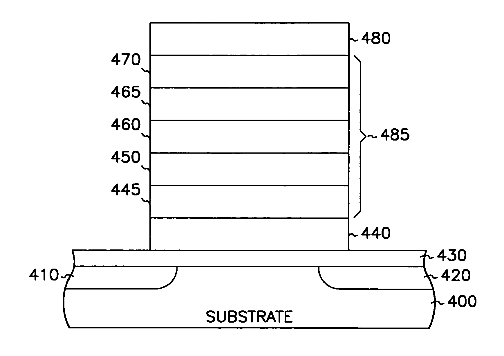
[0018] In the following detailed description of the preferred embodiments, reference is made to the accompanying drawings which form a part hereof, and in which is shown by way of illustration specific preferred embodiments in which the invention may be practiced. These embodiments are described in sufficient detail to enable those skilled in the art to practice the invention, and it is to be understood that other embodiments may be utilized and that logical, mechanical and electrical changes may be made without departing from the spirit and scope of the present inventions. The following detailed description is, therefore, not to be taken in a limiting sense, and the scope of the present invention is defined only by the appended claims.

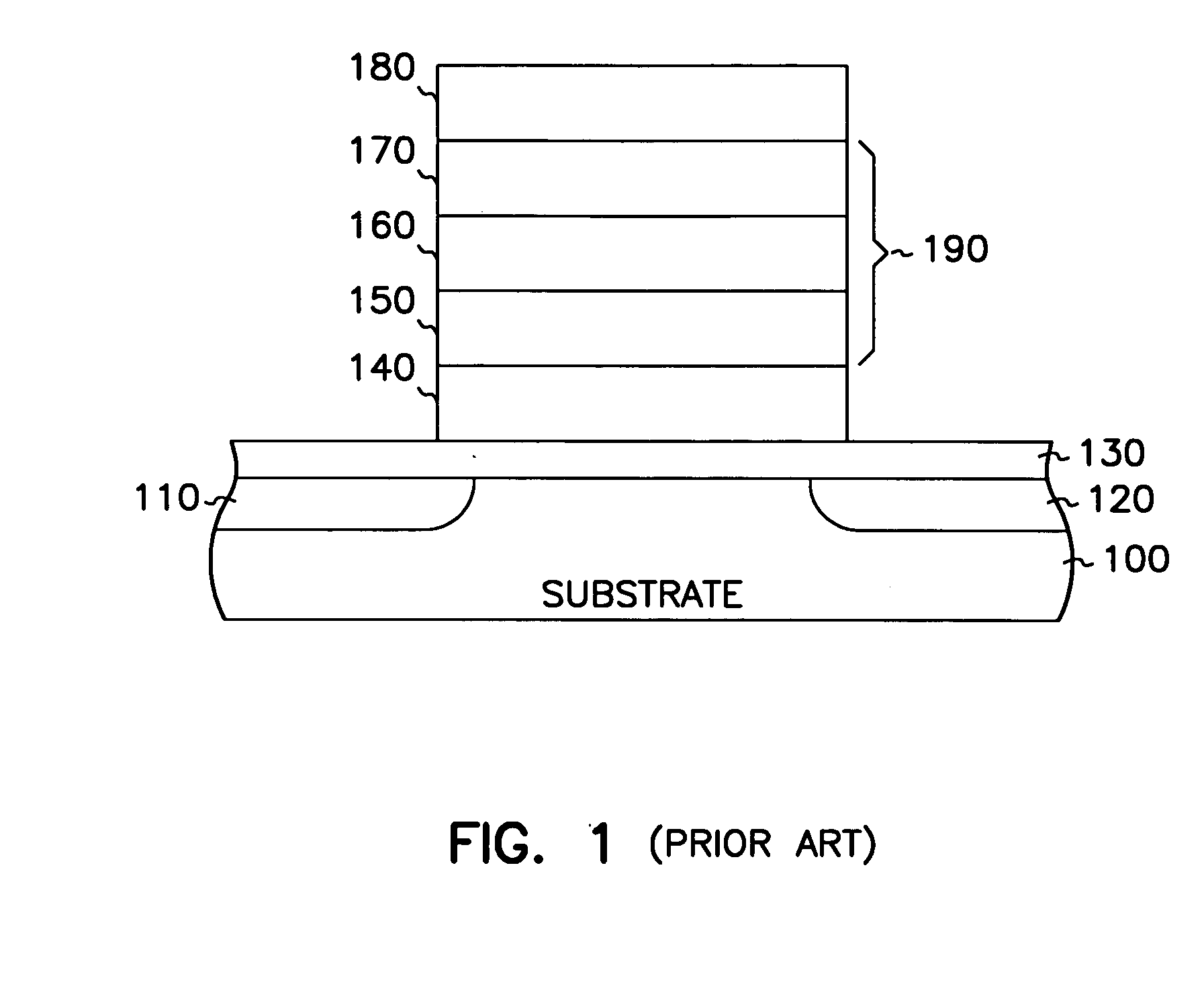
[0019] In one embodiment of the present invention a composite acts as a dielectric in a memory cell of a non-volatile semiconductor memory. Referring to FIG. 1, a block diagram of a prior art memory cell for use in a non-volatile semiconductor memory...


PUM


Abstract

A dielectric insulating composite for insulating a floating gate from a control gate in a non-volatile memory is described. A material, such as an undoped polysilicon, amorphous silicon, or amorphous polysilicon or a silicon rich nitride, is inserted in the gate structure. The oxide film that results from the oxidation of these films is relatively free from impurities. As a result, charge leakage between the floating gate and control gate is reduced.

Description

[0001] This application is a Divisional of U.S. application Ser. No. 10 / 060,451, filed Jan. 30, 2002, which is a Divisional of U.S. application Ser. No. 09 / 233,313, filed Jan. 19, 1999, now U.S. Pat. No. 6,368,919, both of which are incorporated herein by reference.FIELD OF THE INVENTION [0002] This invention relates to the field of semiconductor memories, and more particularly to a method and manufacture for decreasing charge leakage in a non-volatile semiconductor memory. BACKGROUND OF THE INVENTION [0003] The demand for inexpensive, easily accessible and compact long term information storage systems continues to increase. In the past, the demand for long term information storage was met by archiving paper records. Today, however, the volume of information requiring storage makes this solution impractical. Recently, the demand for long term information storage has been met by magnetic media information storage systems and optical information storage systems. Although these systems...

Claims


Application Information

Patent Timeline
Patent Type & Authority Applications(United States)
IPC IPC(8): H01L21/28H01L29/423H01L29/51
CPCH01L21/28273Y10S438/954H01L29/511H01L29/42324H01L29/40114
Inventor NUTTALL, MICHAELMERCALDI, GARRY A.
Owner MICRON TECH INC
Why Eureka
Try Eureka