System and method for manufacturing embedded conformal electronics

a conformal electronics and conformal technology, applied in thermoelectric device manufacturing/treatment, conductive material removal by irradiation, instruments, etc., can solve the problems of affecting component operation, difficult installation, and high cost of such systems, and achieve the effect of enhancing power production

Active Publication Date: 2005-02-10
THE RES FOUND OF STATE UNIV OF NEW YORK
View PDF23 Cites 119 Cited by
  • Summary
  • Abstract
  • Description
  • Claims
  • Application Information

AI Technical Summary

Benefits of technology

[0009] Thermal spray technology coupled with precision laser materials processing has been developed for the fabrication of electronics and sensor fabrication. Thermal spray is implemented for depositing a wide variety of materials that have functional properties as deposited. The materials generally do not need subsequent post-firing, annealing, or other time consuming, costly post processing steps. A variety of materials can be deposited quickly and easily using thermal spray technology. After the deposition, precision laser micromachining using, for example, ultrafast or UV laser systems, can be used to fabricate complex electronic structures. The electronic structures include, for example, resistors, capacitors, coils, transformers, and a variety of sensors, for example, thermistors, thermocouples, thermopiles, strain sensors, magnetic sensors, humidity sensors, gas sensors, flow sensors, heat flux sensors, etc. Furthermore, these sensors can be embedded within a component during manufacture to provide an extremely robust, long-life sensing and health monitoring system for the component, which is superior to aftermarket, add-on sensors that must be attached manually using adhesives or other post-manufacturing techniques. Also, because the thermal spray technique is self-compatible, it can be used to fabricate three-dimension electronics and sensor systems, e.g., multi-layer sensors on the same surface area footprint, multiple-layer thermopiles for enhanced power production, etc.

Problems solved by technology

As a consequence, however, these very same engineering systems are becoming extremely complex, with the result that the costs involved to repair such systems, particularly for major component failures, are skyrocketing.
However, after-market sensors, even if attached during the manufacturing process, can be unreliable, difficult to install, and may adversely affect component operation.
Electronic manufacturing with feature sizes in the meso-scale regime (e.g., about 10 to 1000 micrometers) often needs multi-step processes that include time-consuming photolithographic methodologies.
The high temperature curing process gives rise to issues associated with mismatch in thermal expansion between dissimilar materials and can lead to premature debonding.
Current screen printing technology is inherently limited in its fine feature capabilities, with the line width being limited to 100 microns or higher.

Method used


Image

  • System and method for manufacturing embedded conformal electronics
  • System and method for manufacturing embedded conformal electronics
  • System and method for manufacturing embedded conformal electronics

Examples


Embodiment Construction

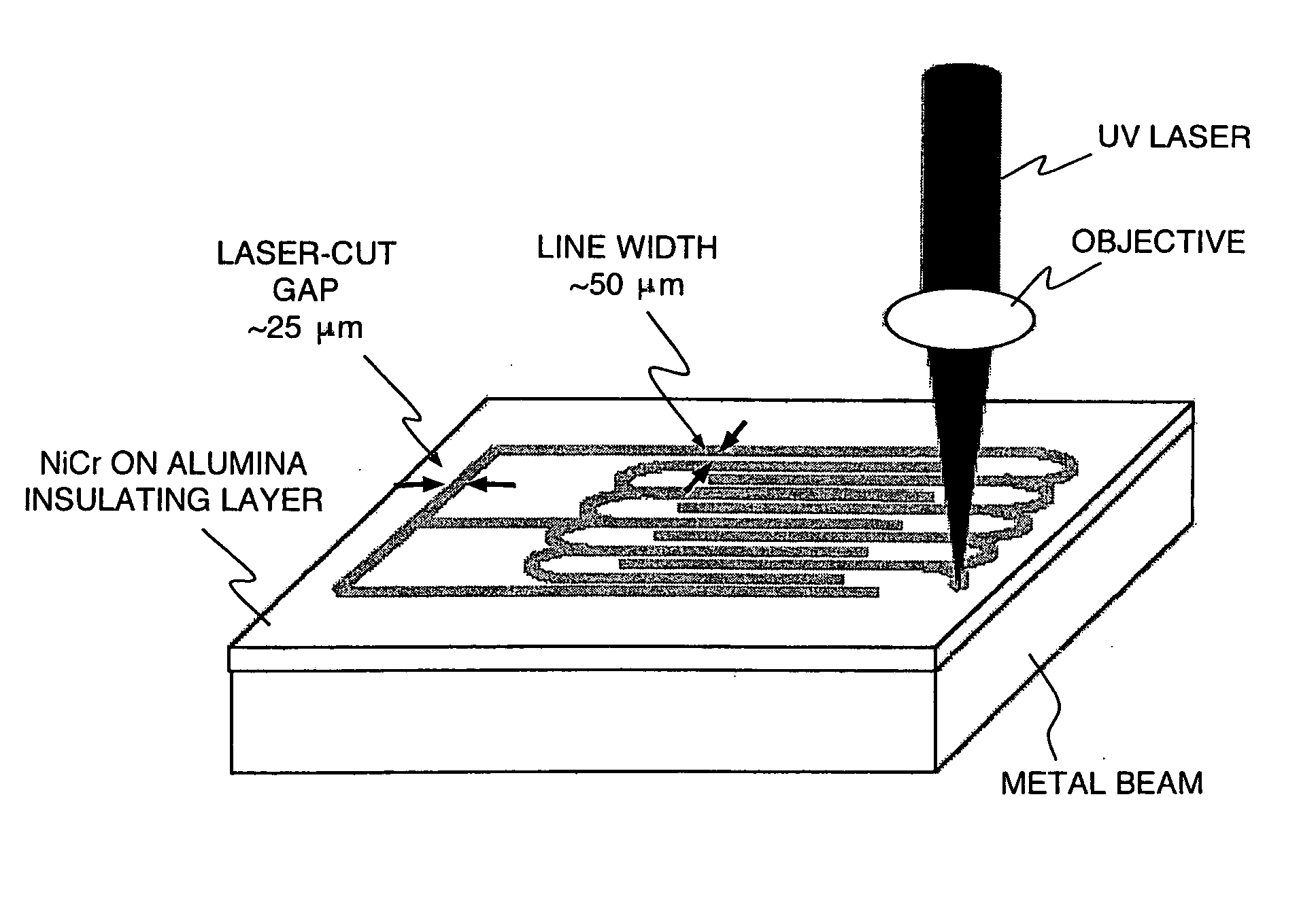
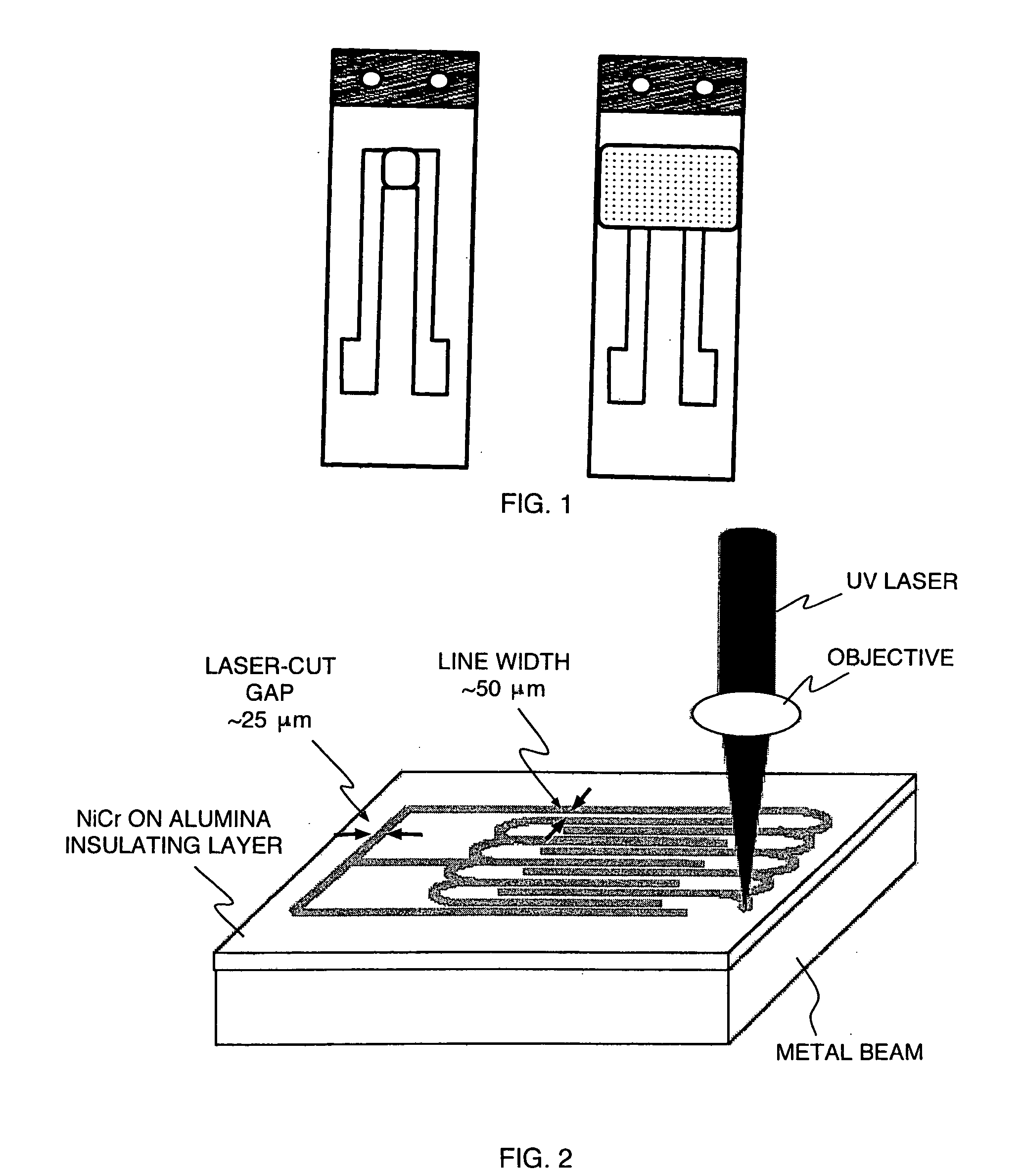
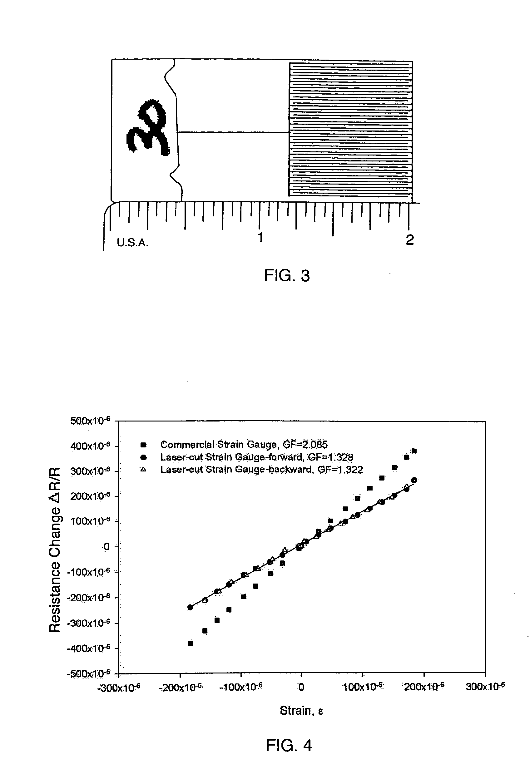
[0038] Direct write electronics technologies provide an opportunity to integrate mesoscopic electronic devices with the physical structure on which the electronic systems will be used, eliminating the need for a traditional printed circuit board. The ability to print electronic features on flexible and conformal substrates enables unique applications for deployable electronics, such as placing electronics in projectiles, for flexible satellite solar arrays, usage in rolled-up forms that can be inserted into symmetric or odd shapes, installed on military gear, as well as various surveillance equipment. This can save space and reduce weight through 3-D integration. It can provide a dramatic cost savings by eliminating the majority of passive components in automated fabrication, while minimizing procurement. It can reduce inventories of electronic components or parts, enable the building of specialty parts on the “fly” without mass production set-up costs, and increase the reliability ...


PUM

PropertyMeasurementUnit
sizesaaaaaaaaaa
widthaaaaaaaaaa
wavelengthaaaaaaaaaa

Abstract

A method for fabricating an electronic device comprises providing a substrate (501), direct writing a functional material by a thermal spray on the substrate (502) and removing a portion of the function material to form the electronic or sensory device (503).

Description

[0001] The U.S. Government has a paid-up license in this invention and the right in limited circumstances to require the patent owner to license others on reasonable terms as provided for by the terms of grant no. N000140010654, awarded by the Department of Defense, DARPA.BACKGROUND OF THE INVENTION [0002] 1. Field of the Invention [0003] The present invention relates to conformal electronic devices, and more particularly to a method of fabricating conformal electronics using additive-subtractive techniques. [0004] 2. Discussion of the Prior Art [0005] The adoption of computer-based design, engineering, and analysis tools over the past 10-20 years has resulted in a tremendous acceleration in the development cycle of modern engineering systems. Modern engineering systems are lighter, smaller, last longer, are more efficient, and are far more reliable than their predecessors of even a few years ago. As a consequence, however, these very same engineering systems are becoming extremely ...

Claims


Application Information

Patent Timeline
Patent Type & Authority Applications(United States)
IPC IPC(8): B23K26/36C23C4/18G03F7/20H01L21/768
CPCH01L21/76838G03F7/70383H01L35/32H01L35/34H05K3/027H05K3/04H05K3/043H05K3/14H05K2203/1344B23K26/0093B23K26/365B23K2201/36C23C4/18C23C4/185H01L21/76894B23K26/361B23K2101/36H10N10/01H10N10/17
Inventor GAMBINO, RICHARDLONGTIN, JONSAMPATH, SANJAY
Owner THE RES FOUND OF STATE UNIV OF NEW YORK
Why Eureka
Try Eureka