Pixel for a fringe field switching reflective and transflective liquid crystal display

a liquid crystal display and fringe field technology, applied in optics, instruments, transistors, etc., can solve the problems of increasing manufacturing costs, too large optical-path differences, limited viewing angle of display, etc., to reduce mask steps to manufacture, improve the efficiency of reflecting light, and reduce manufacturing costs

Inactive Publication Date: 2005-02-10
WISTRON OPTRONICS CORP
View PDF5 Cites 53 Cited by
  • Summary
  • Abstract
  • Description
  • Claims
  • Application Information

AI Technical Summary

Benefits of technology

[0005] Another object of the present invention is to provide a pixel for an FFS-LCD with reduced mask steps to manufacture therefore.
[0006] In a pixel for an FFS-LCD, according to the present invention, on a substrate an ultra-micro scattering layer with a top surface in a nano-scale roughness resulted from the crystallization or the property of the material within the ultra-micro scattering layer is formed, and a reflective layer is then formed on the ultra-micro scattering layer to be conformal to the top surface, so as to obtain a reflective surface in a

Problems solved by technology

When the reflector for an LCD is made of metal, the reflective surface is so smooth that mirror-like reflection is occurred for the light reflected by that reflector, and thus the viewing angle of the display is limited.
However, to introduce the organic layer requires more mask steps, and thus the total mask steps to manufacture an LCD need about 8˜10 masks, whe

Method used


Image

  • Pixel for a fringe field switching reflective and transflective liquid crystal display
  • Pixel for a fringe field switching reflective and transflective liquid crystal display
  • Pixel for a fringe field switching reflective and transflective liquid crystal display

Examples


first embodiment

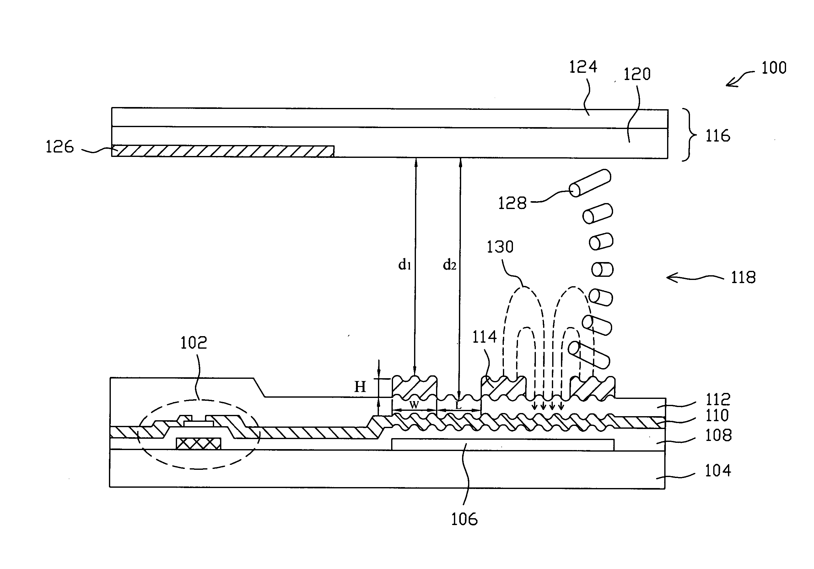
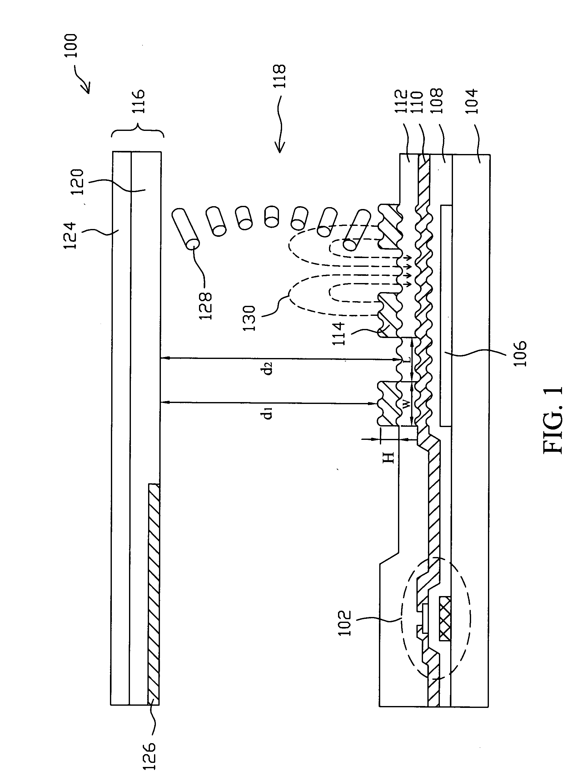
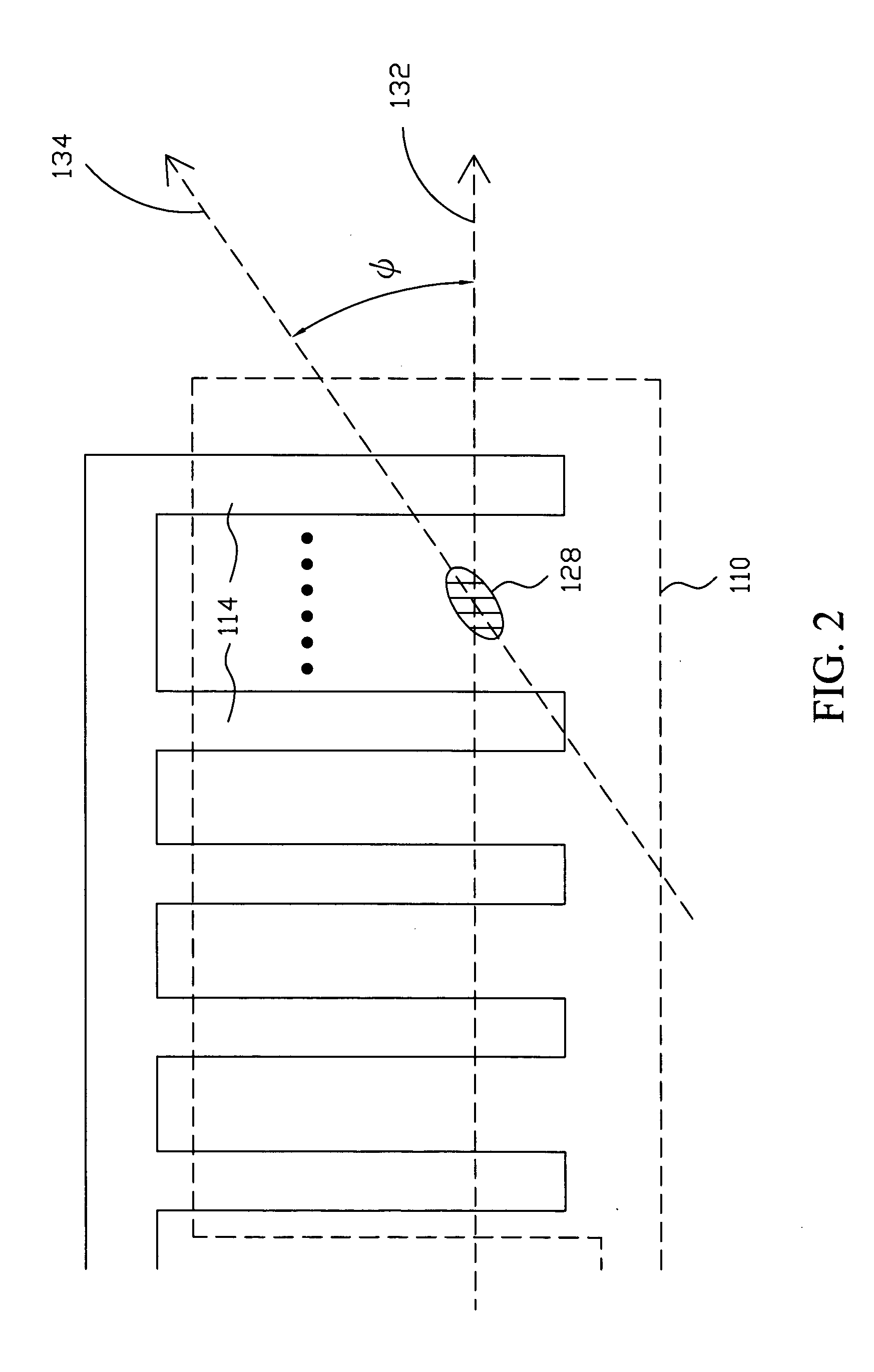
[0021]FIG. 4 shows a schematic diagram of the cross-sectional view of first embodiment pixel 200 for a transflective LCD according to the present invention, which is similar to the pixel 100 shown in FIG. 1, and comprises a thin-film transistor 102 on a substrate 104, a transparent conductive layer 106 with an insulator layer 108 and a passivation layer 112 thereon, a reflective layer including several metal stripes 114, and a layer 118 of liquid crystal molecules 128 with a horizontal rubbing direction sandwiched between the reflective layer 114 and an optical stack 116 including a color filter 120 and a polarizer 124. However, the pixel 200 employs a transparent conductive layer 202 to replace the metal layer 110 of the pixel 100 shown in FIG. 1. Likewise, when the insulator layer 108 is formed on the transparent conductive layer 106, due to the property of the material to form the insulator layer 108, its top surface will become of a nano-scale roughness simultaneously, and by wh...

second embodiment

[0024]FIG. 5 shows a schematic diagram of the cross-sectional view of second embodiment pixel 210 for a transflective LCD according to the present invention, which comprises a thin-film transistor 102 on a substrate 104, an ultra-micro scattering layer including a transparent conductive layer 106 and an insulator layer 108, a passivation layer 112, a reflective layer including several metal stripes 114, a layer 118 of liquid crystal molecules 128 with a horizontal rubbing direction sandwiched between the reflective layer 114 and an optical stack 116 including a color filter 120 and a polarizer 124, and a black matrix 126 at the front end of the color filter 120 to shield the thin-film transistor 102. In the pixel 210, the thin-film transistor 102 and the ultra-micro scattering layer are arranged on the substrate 104, and the reflective layer 114 is formed on the ultra-micro scattering layer and is formed of the same metal layer to implement the source / drain of the thin-film transist...

third embodiment

[0025]FIG. 6 shows a schematic diagram of the cross-sectional view of third embodiment pixel 300 for a transflective LCD according to the present invention, which comprises a thin-film transistor 302 on a substrate 304, an insulator layer 306 on the substrate 304, an ultra-micro scattering layer including a transparent conductive layer 308 and an insulator layer 310 with the transparent conductive layer 308 sandwiched between the two insulator layers 306 and 310 and formed of the same metal layer to manufacture the drain 3022 of the thin-film transistor 302, a reflective layer 312 including several high reflective metal stripes on the insulator layer 310, an optical stack 314, and a layer 316 of liquid crystal molecules 128 arranged between the optical stack 314 and the reflective layer 312. The optical stack 314 includes a color filter 318 and a polarizer 322, and a black matrix 324 is disposed at the front end of the color filter 318. The insulator layer 310 is made of for example...


PUM


Abstract

By employing an ultra-micro scattering layer with a top surface in a nano-scale roughness resulted from the crystallization or the property of the material within the ultra-micro scattering layer in a pixel for a fringe field switching liquid crystal display, the mask steps to manufacture the liquid crystal display and the cost therefore are reduced. The nano-scale roughness of the top surface on the ultra-micro scattering layer results in larger scattering angle and smooth distribution for the scattering effect. Accordingly, the reflectivity will not vary violently with the viewing angle, and excellent anti-glare effect is obtained also.

Description

FIELD OF THE INVENTION [0001] The present invention relates generally to a fringe field switching (FFS) liquid crystal display (LCD) and more particularly, to a pixel for an FFS-LCD with a nano-scale rough surface thereof and without more mask steps to manufacture therefore. BACKGROUND OF THE INVENTION [0002] In a conventional FFS-LCD, the electrode is made of ITO and in transmissive manner for the modulated light to pass therethrough, and on the other hand, the typical reflective twisted nematic (RTN) TFT-LCD employs metal to implement the reflector thereof for the light to be reflected thereby. When the reflector for an LCD is made of metal, the reflective surface is so smooth that mirror-like reflection is occurred for the light reflected by that reflector, and thus the viewing angle of the display is limited. To enhance the scattering effect to the light, an organic layer such as resin is introduced under the reflector so as to result in roughness on the reflective surface. Howe...

Claims


Application Information

Patent Timeline
IPC IPC(8): G02F1/1333G02B5/02G02F1/1335G02F1/1343G02F1/1368
CPCG02F1/133504G02F1/134363G02F1/133553G02F1/133555H01L29/786G02F1/134372
Inventor LIU, HONG-DA
Owner WISTRON OPTRONICS CORP
Why Eureka
Try Eureka