Filling vias with thick film paste using contact printing

a contact printing and via technology, applied in the manufacture of resistive materials, electrode systems, electric discharge tubes/lamps, etc., can solve the problems of invariably running off of screen printed film, incomplete and uneven filling of vias or slots of fine dimensions, and finite thickness of screen printed film. , to achieve the effect of preventing paste run-o

Inactive Publication Date: 2005-02-10
EI DU PONT DE NEMOURS & CO
View PDF14 Cites 14 Cited by
  • Summary
  • Abstract
  • Description
  • Claims
  • Application Information

AI Technical Summary

Benefits of technology

[0022] In one embodiment, the coating edge comprises one or more wings on either end, which are in contact with the top surface. The wings are perpendicular to the coating edge and serve the purpose of preventing paste run-off. The wing may be formed from any suitable material including such materials as metals, plastics and like material.
[0023] In another embodiment the thick film paste may be printed where a coating edge is parallel rather than orthogonal to the via side (edge) of greatest length. This results in more deposition of material in the vias.

Problems solved by technology

Firstly, since the thick film paste must be squeezed through the fine mesh of a screen, the shadow marks of the screen mesh are always present in the printed paste film.
These mesh marks can lead to incomplete and uneven filling of vias or slots of fine dimensions.
Secondly, the screen printed film has a finite thickness and will invariably over fill the vias or slots on the substrate.
Thirdly, since the vias or slots areas on the substrate typically represents only 2 to 10% of the total printed area, a large excess of paste is used with conventional screen printing.
This excess amount of paste not only leads to significantly higher material cost, but also results in longer drying time and greater difficulty in removing all excess paste from unwanted area.

Method used


Image

  • Filling vias with thick film paste using contact printing
  • Filling vias with thick film paste using contact printing
  • Filling vias with thick film paste using contact printing

Examples


example 1

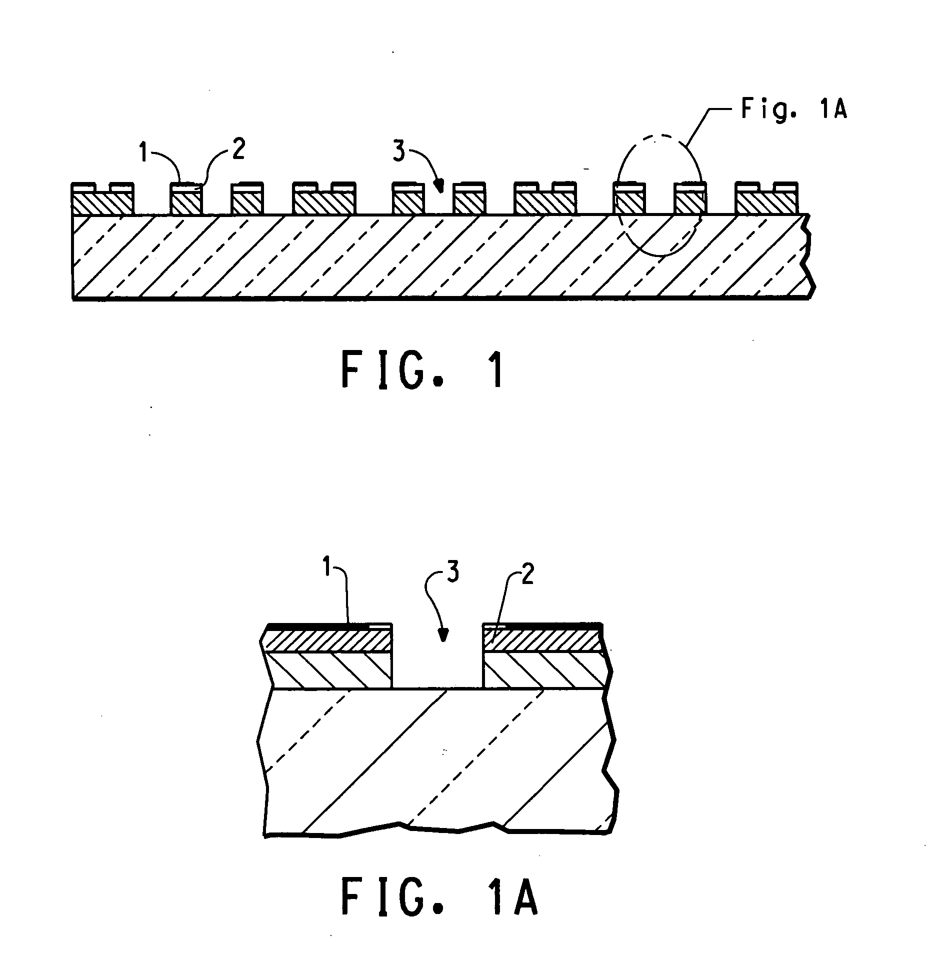
[0062] This example demonstrates the disadvantages of using conventional screen printing to fill fine dimension vias with a thick film paste as part of a process to fabricate an electron field emission device.

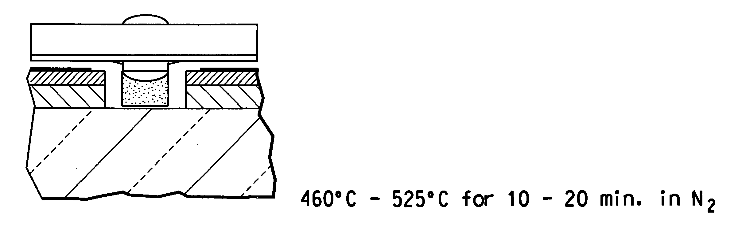
[0063] A glass substrate coated with an in-situ chromium photomask was prepared by first sputtering a layer of Cr of about 2000 A on the glass substrate. The Cr layer was patterned with arrays of 20 μm circles where the Cr coating was etched out. A novalac type photoresist, AZ4620 obtained from Clariant Cooperation of Sulzbach am Taunus, Germany, was spin coated on the Cr coated side of the glass substrate. A spinning speed of 1000 rpm and a spinning time of 45 seconds were used. The novalac polymer film was dried on a 95° C. hot plate for 10 minutes. A 12 μm thick novalac polymer film was obtained after drying. The photoresist was exposed to UV (350-450 nm) radiation through the in-situ Cr photomask from the back side of the substrate. A UV dose of 400 mJ / cm2 was used. The ph...

example 2

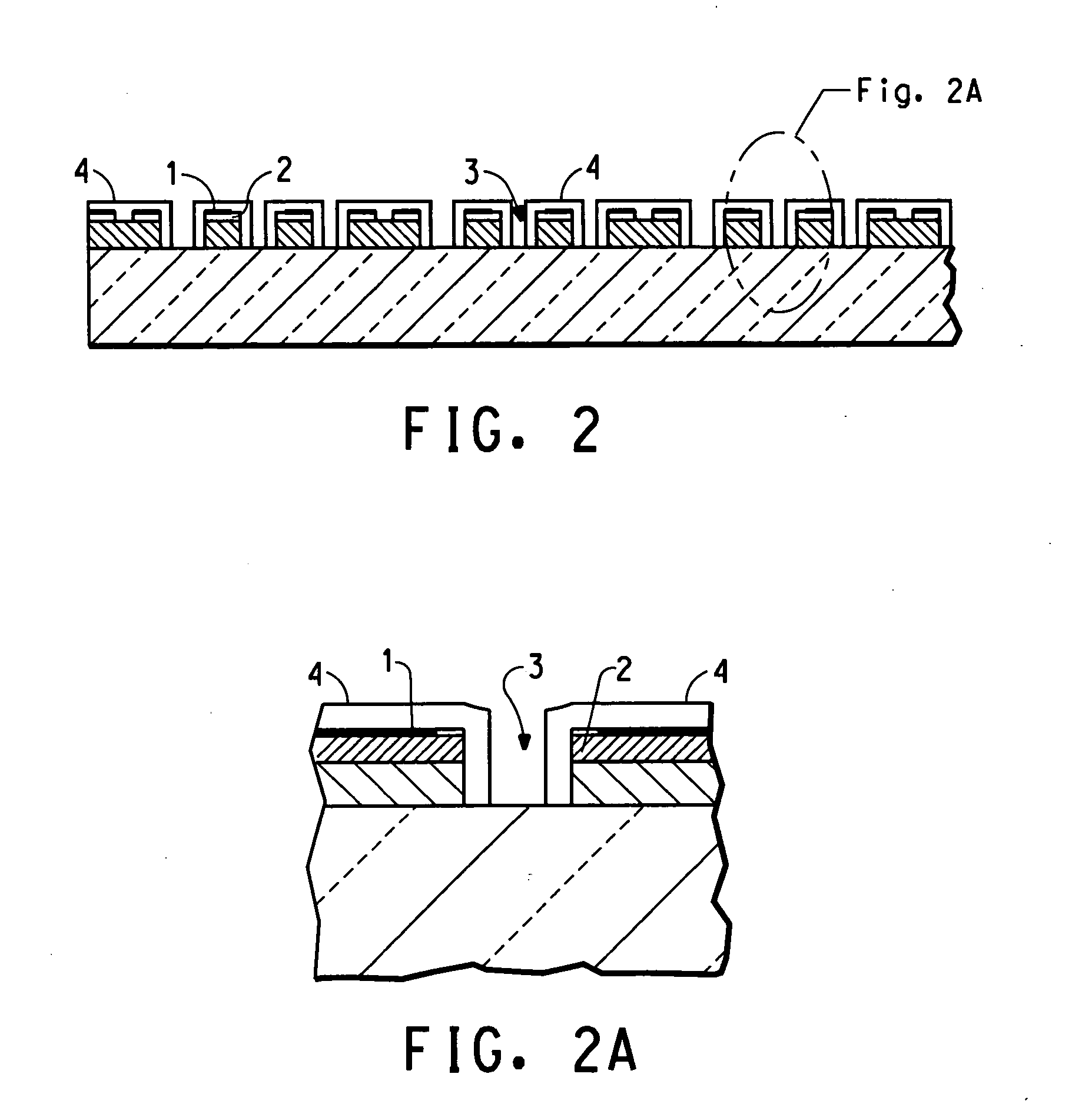
[0068] This example describes the contact printing process and illustrates the benefits of using contact printing for filling vias with a photoimagable thick film paste containing carbon nanotubes.

[0069] As in Example 1, a glass substrate coated with an in-situ Cr photomask patterned with an array of open circles of 20 μm was prepared. A novalac type photoresist, AZ4620 obtained from the Clariant Cooperation, was spin coated on the Cr coated side of the glass substrate. A spinning speed of 1000 rpm and a spinning time of 45 seconds were used. The novalac polymer film was dried on a 95° C. hot plate for 10 minutes. A 12 μm thick novalac polymer film was obtained after drying. The photoresist was exposed to UV (350-450 nm) radiation through the in-situ Cr photomask from the back of the substrate. A UV dose of 400 mJ / cm2 was used. The photoresist was developed in AZA21 K developer solution also obtained from Clariant for 45 seconds. Post development, the substrate was baked on a 120° ...


PUM

PropertyMeasurementUnit
diameteraaaaaaaaaa
diameteraaaaaaaaaa
diameteraaaaaaaaaa

Abstract

The present invention relates to a process for filling vias in an electronic structure with thick film paste. The vias may be preexisting in a substrate comprised of thick film materials or fabricated in a photoresist layer over-coating the substrate. The invention is particularly useful in fabrication of electron field emission triode arrays where the vias are of fine dimension (<100 μm in diameter) and the electron emitter thick film paste, which may contain carbon nanotubes, is of high value.

Description

FIELD OF THE INVENTION [0001] The present invention relates to a process for filling vias in an electronic structure with thick film paste. The invention is particularly useful in fabrication of electron field emission triode arrays where the vias are of fine dimension (<100 μm in diameter) and the electron emitter thick film paste, which may contain carbon nanotubes, is of high value. TECHNICAL BACKGROUND [0002] Bouchard et al (WO 01 / 99146) describe a field emitter thick film paste composition, a process of application of said thick film paste by conventional screen printing and photoimaging, as well as a process for improving the field emitter. [0003] The use of conventional screen printing however presents several disadvantages. Firstly, since the thick film paste must be squeezed through the fine mesh of a screen, the shadow marks of the screen mesh are always present in the printed paste film. These mesh marks can lead to incomplete and uneven filling of vias or slots of fin...

Claims


Application Information

Patent Timeline
Patent Type & Authority Applications(United States)
IPC IPC(8): B05D5/12H01J1/304H01J9/02H01L21/00H05K3/00H05K3/10H05K3/40H05K3/46
CPCB82Y10/00H01J1/304H01J9/025H01J2201/30469H05K2203/0514H05K3/4069H05K3/4664H05K2203/0139H05K3/0023
Inventor CHENG, LAP-TAK ANDREWBEIKMOHAMADI, ALLAN
Owner EI DU PONT DE NEMOURS & CO
Why Eureka
Try Eureka