Method for fabricating high frequency module

a high-frequency module and manufacturing method technology, applied in the direction of semiconductor devices, semiconductor/solid-state device details, electrical apparatus, etc., can solve the problems of increasing the overall power consumption, the size and weight of the communication terminal device, and the insufficient properties of the conventional high-frequency transmitter-receiver circuit to meet the requirements, so as to achieve the effect of small size and cost reduction

Inactive Publication Date: 2005-02-17
SONY CORP
View PDF2 Cites 30 Cited by
  • Summary
  • Abstract
  • Description
  • Claims
  • Application Information

AI Technical Summary

Benefits of technology

[0039] In the method for manufacturing a high-frequency module device according to this invention, since the high-frequency circuit unit is formed on the flattened one surface of the dummy board, a high-frequency module device in which the wiring layer having the passive element is accurately formed can be manufactured.
[0040] Moreover, in this m...

Problems solved by technology

Therefore, the high-frequency transmitter-receiver circuit 100 has a large size as a whole, which is a big problem in reducing the size and weight of the communication terminal device.
Therefore, the high-frequency transmitter-receiver circuit 110 has a problem that a DC offset cancellation circuit and a low-pass filter are needed, increasing the overall power consumption.
Whether the superheterodyne system or the direct conversion system, the conventional high-frequency transmitter-receiver circuit does not have sufficient properties to meet the requirements such as reduction in size and weight of the communication terminal device.
In this high-frequency circuit board, since the process of forming the inductor includes many steps and is complex, there is a problem of increase in the manufacturing cost.
In this high-frequency circuit board, electrical interference of the Si substrate exis...

Method used


Image

  • Method for fabricating high frequency module
  • Method for fabricating high frequency module
  • Method for fabricating high frequency module

Examples


Embodiment Construction

[0070] Hereinafter, the method for manufacturing a high-frequency module device according to this invention will be described with reference to the drawings.

[0071] First, a high-frequency module device manufactured by the manufacturing method according to this invention will be described with reference to FIG. 8.

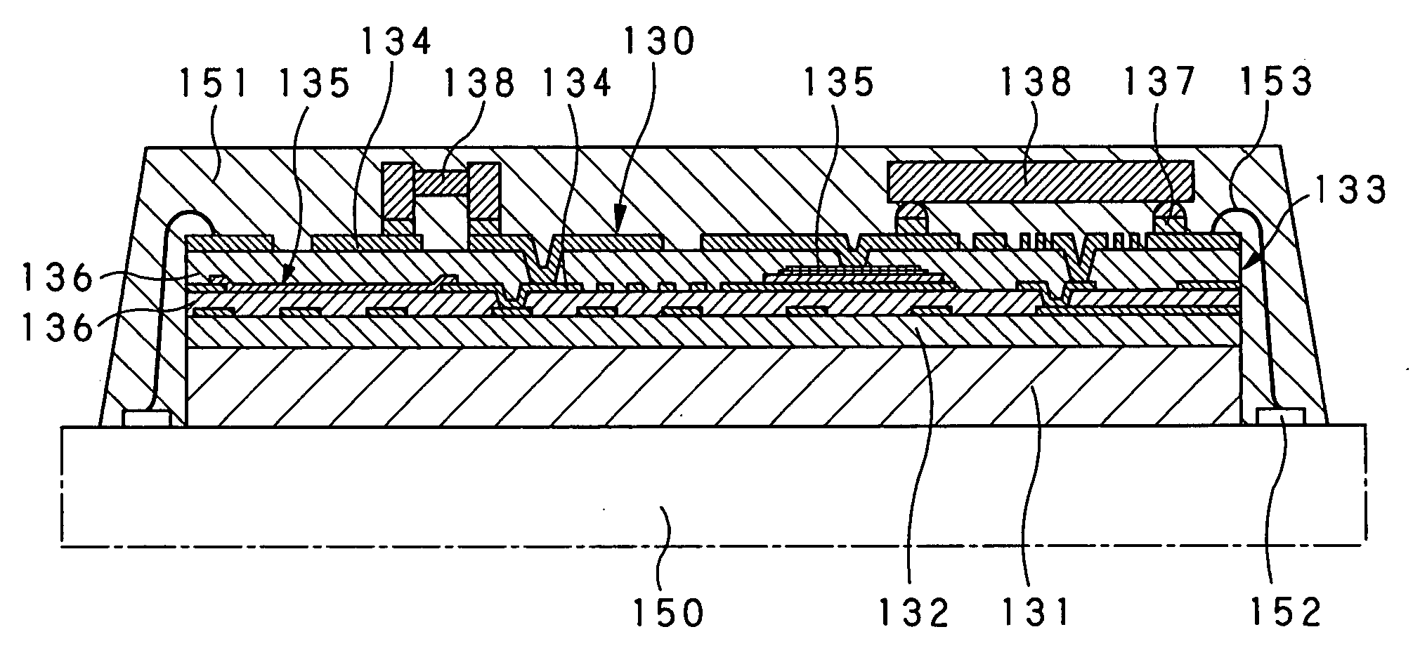
[0072] A high-frequency module device 1 shown in FIG. 8 constitutes a high-frequency circuit for performing exchange processing or the like of a high-frequency signal using a superheterodyne system, direct conversion system or the like in a transmitter-receiver unit provided in a portable communication terminal device or the like.

[0073] This high-frequency module device 1 has a structure in which a high-frequency circuit board having a high-frequency circuit unit 2 formed thereon is electrically connected and mounted on a base board 3 with a bump part 4 made of, for example, solder or the like. In this high-frequency circuit unit 2, a second unit wiring layer 6 is formed ...


PUM


Abstract

This invention is a method for manufacturing a high-frequency module device. A high-frequency circuit unit (2) in which first to third unit wiring layers (5) to (7), each having a capacitor (12) or the like at a part, are stacked and formed on flattened one surface of a dummy board (30) so that a third pattern wiring is exposed from a connection surface (2a) of an uppermost layer is mounted on a mounting surface (3a) of a base board (3) where an input/output terminal part (18) is exposed, in such a manner that the third pattern wiring and the input/output terminal part are connected with each other, and after that, the dummy board is removed. A high-frequency module device is thus manufactured.

Description

TECHNICAL FIELD [0001] This invention relates to a method for manufacturing a high-frequency module device having a high-frequency circuit unit on which a passive element is provided, and particularly to a method for manufacturing a high-frequency module device with reduced size and thickness. [0002] This application claims priority of Japanese Patent Application No. 2002-286837, filed on Sep. 30, 2002, the entirety of which is incorporated by reference herein. BACKGROUND ART [0003] Conventionally, digitization of data has enabled easy handling of various information such as music, sounds and images by a personal computer, mobile computer and the like. An audio codec technique and a video codec technique have realized band compression of such information, and an environment for easily and efficiently distributing the information to various communication terminal devices via digital communication or digital broadcasting is almost complete. For example, audio and video data (AV data) ...

Claims


Application Information

Patent Timeline
IPC IPC(8): H01L23/12H01L23/498H01L23/538H01L23/64
CPCH01L23/49833H01L2224/16235H01L23/642H01L23/645H01L2221/68345H01L2221/68363H01L2224/16225H01L2224/48091H01L2224/73253H01L2924/01078H01L2924/01079H01L2924/09701H01L2924/16152H01L2924/19041H01L2924/19105H01L2924/19107H01L2924/30107H01L2924/3025H01L23/5389H01L24/48H01L2924/00014H01L2224/16237H01L2224/16238H01L2924/12042H01L2924/14H01L2924/181H01L2924/00H01L2924/00012H01L2224/45099H01L2224/45015H01L2924/207H01L23/12H01P1/20
Inventor OGAWA, TSUYOSHIKOSEMURA, TAKAHIKOMUTO, AKIRAOKUBORA, AKIHIKO
Owner SONY CORP
Why Eureka
Try Eureka