
Method of etching and etching apparatus

a technology of etching apparatus and etching method, which is applied in the direction of electrical equipment, basic electric elements, semiconductor/solid-state device manufacturing, etc., can solve the problems of preventing degradation of the capability to etch a target, and the etching time becomes longer, so as to achieve excellent controllability, increase the etching selectivity of silicon oxide film against silicon nitride film of the gate, and excellent controllability

Inactive Publication Date: 2005-02-24
TOKYO ELECTRON LTD
View PDF12 Cites 22 Cited by
  • Summary
  • Abstract
  • Description
  • Claims
  • Application Information

AI Technical Summary

Benefits of technology

[0007] Therefore, the present invention has been made to ameliorate the above-described disadvantages in the prior arts and an object of the present invention is to provide a novel and improved etching method and etching apparatus thereof assuring an excellent controllability, in which etching selectivity of a silicon oxide film layer against a silicon nitride film layer of a gate can be increased. Thereby, the silicon nitride film layer, acting as a protective film layer of the gate, can be strongly prevented from being etched while it becomes possible to form a contact hole with a high aspect ratio possible.
[0016] In accordance with the present invention as described above, it is possible to increase the etching rate of the silicon oxide film acting as an insulating film layer, while preventing an etching stop from occurring. Further, it is possible to improve etching selectivity of the silicon oxide film over the silicon nitride film, acting as a protective film layer of a gate. Therefore, the silicon nitride film, acting as the protective film layer of the gate, is prevented from being etched and a contact hole with a high aspect ratio may be stably formed while assuring an excellent controllability. Thereby, the present invention satisfies recent demands for improved integration of a semiconductor device and miniaturization of various elements formed on a semiconductor substrate.

Problems solved by technology

However, the plasma etching employing the conventional processing gases as described above is disadvantageous in that as the aspect ratio of the contact hole becomes higher, because of the narrow gaps between the gates, the etching time becomes longer to prevent degradation of the capability to pierce an etching target and occurrence of an etching stop.

Method used


Image

  • Method of etching and etching apparatus
  • Method of etching and etching apparatus
  • Method of etching and etching apparatus

Examples


Embodiment Construction

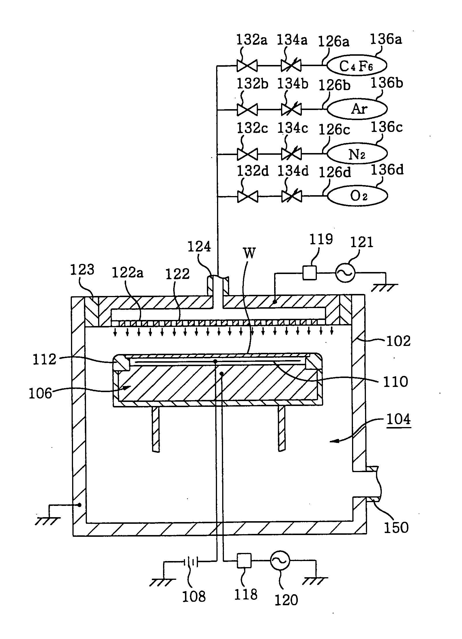
[0023] Hereinafter, preferred embodiments of an etching method and an etching apparatus in accordance with the present invention will now be described in detail with reference to the accompanying drawings. FIG. 1 schematically illustrates a parallel plate type plasma etching apparatus, which is an embodiment of the etching apparatus in accordance with the present invention.

[0024] The plasma etching apparatus 100 includes a processing chamber 104 defined by a securely grounded processing vessel 102, and a vertically movable lower electrode 106 included in a suscepter is installed in the processing chamber 104. An electrostatic chuck 110 connected to a high voltage DC power supply 108 is provided at an upper part of the lower electrode 106 and an object to be processed, for example a semiconductor wafer (hereinafter, referred to as “wafer”) W, is loaded on the electrostatic chuck 106. Further, an insulating focus ring 112 is installed around the wafer W loaded on the lower electrode ...


PUM


Abstract

Silicon oxide film having, as a sublayer, a silicon nitride film layer serving as a protective film layer for gate formed on silicon substrate is etched by introducing a processing gas including a gaseous mixture containing at least C4F6, Ar, O2 and N2 into an airtight processing chamber and carrying out a plasma treatment in a self-alignment contact process, thereby forming contact hole. For the processing gas, e.g., the ratio of N2 gas flow rate to C4F6 gas flow rate ranges from 25 / 8 to 85 / 8, the ratio of O2 and N2 gas flow rate to C4F6 gas flow rate ranges from 15 / 4 to 45 / 4 and the ratio of N2 gas flow rate to O2 gas flow rate ranges from 5 to 17. Accordingly, stable contact holes of high aspect ratio exhibiting desirable control characteristics is formed while minimizing etching the silicon nitride film, a protective film layer for gate.

Description

[0001] This application is a Continuation Application of PCT International Application No. PCT / JP03 / 02870 filed on Mar. 11, 2003, which designated United States.FIELD OF THE INVENTION [0002] The present invention relates to an etching method and an etching apparatus, employed to a manufacturing process of a semiconductor device. BACKGROUND OF THE INVENTION [0003] As shown in FIG. 4, in case of forming a contact hole 20 by a plasma etching through an insulating film layer 16, which covers a gate 12 formed on a semiconductor substrate 10 such as a silicon substrate, and is made of a silicon oxide film such as SiO2, a self-alignment contact technology may be applied. In the self-alignment contact technology, the contact hole 20 is formed in a self-aligning manner in a small and compact area between gates 12 while a protective film layer 14 such as a silicon nitride (SiN) film is formed on each gate 12, thereby preventing the gate 12 from being etched in the course of forming the contac...

Claims


Application Information

Patent Timeline
IPC IPC(8): H01L21/311H01L21/60H01L21/3065
CPCH01L21/76897H01L21/31116
Inventor KOBAYASHI, NORIYUKIADACHI, KENJI
Owner TOKYO ELECTRON LTD
Learn More