Optimization of routing layers and board space requirements for ball grid array package implementations including array corner considerations

a technology of array corners and routing layers, applied in the direction of printed circuit aspects, program control, instruments, etc., can solve the problems of not fully populated array perimeters with conductive pads, and the array perimeters are not fully populated with conductive pads, so as to improve the signal routing of integrated circuit packages and improve the land pattern for attaching the ic packages. , the effect of improving the contact pad array

Inactive Publication Date: 2005-02-24
AVAGO TECH INT SALES PTE LTD
View PDF6 Cites 10 Cited by
  • Summary
  • Abstract
  • Description
  • Claims
  • Application Information

AI Technical Summary

Benefits of technology

The present invention provides a method and apparatus for improving signal routing of integrated circuit (IC) packages and printed circuit boards (PCBs). The present invention further provides improved contact pad arrays for IC packages, and improved land patterns for attaching the IC packages. The land patterns and arrays are formed with edge rows that are not fully populated with contact pads. Spaces in the non-fully populated edge rows allow for additional signal routing channels, which eases IC package and PCB design and manufacturing and improves performance.

Problems solved by technology

One or more edges of a perimeter of the array is not fully populated with conductive pads.

Method used


Image

  • Optimization of routing layers and board space requirements for ball grid array package implementations including array corner considerations
  • Optimization of routing layers and board space requirements for ball grid array package implementations including array corner considerations
  • Optimization of routing layers and board space requirements for ball grid array package implementations including array corner considerations

Examples


Embodiment Construction

Overview

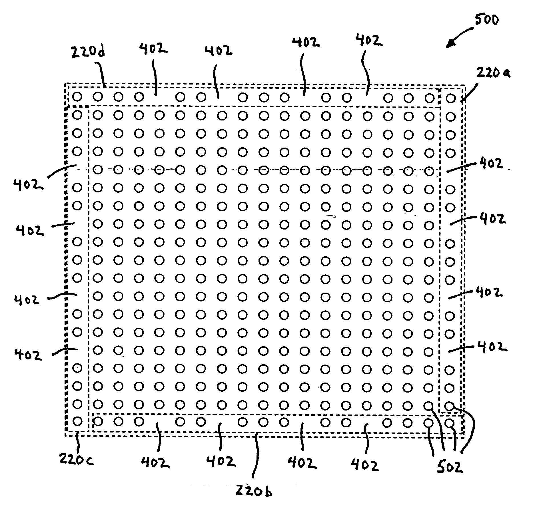
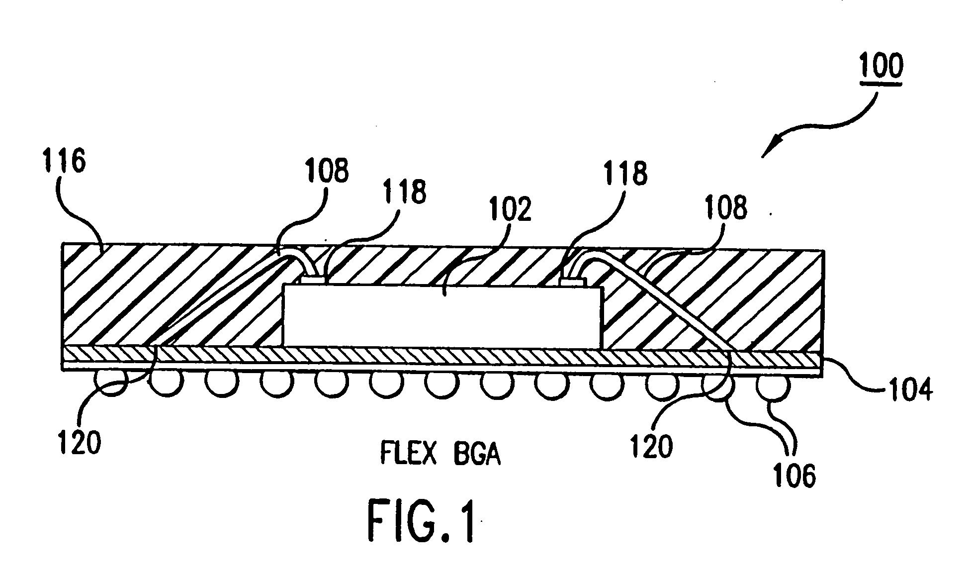
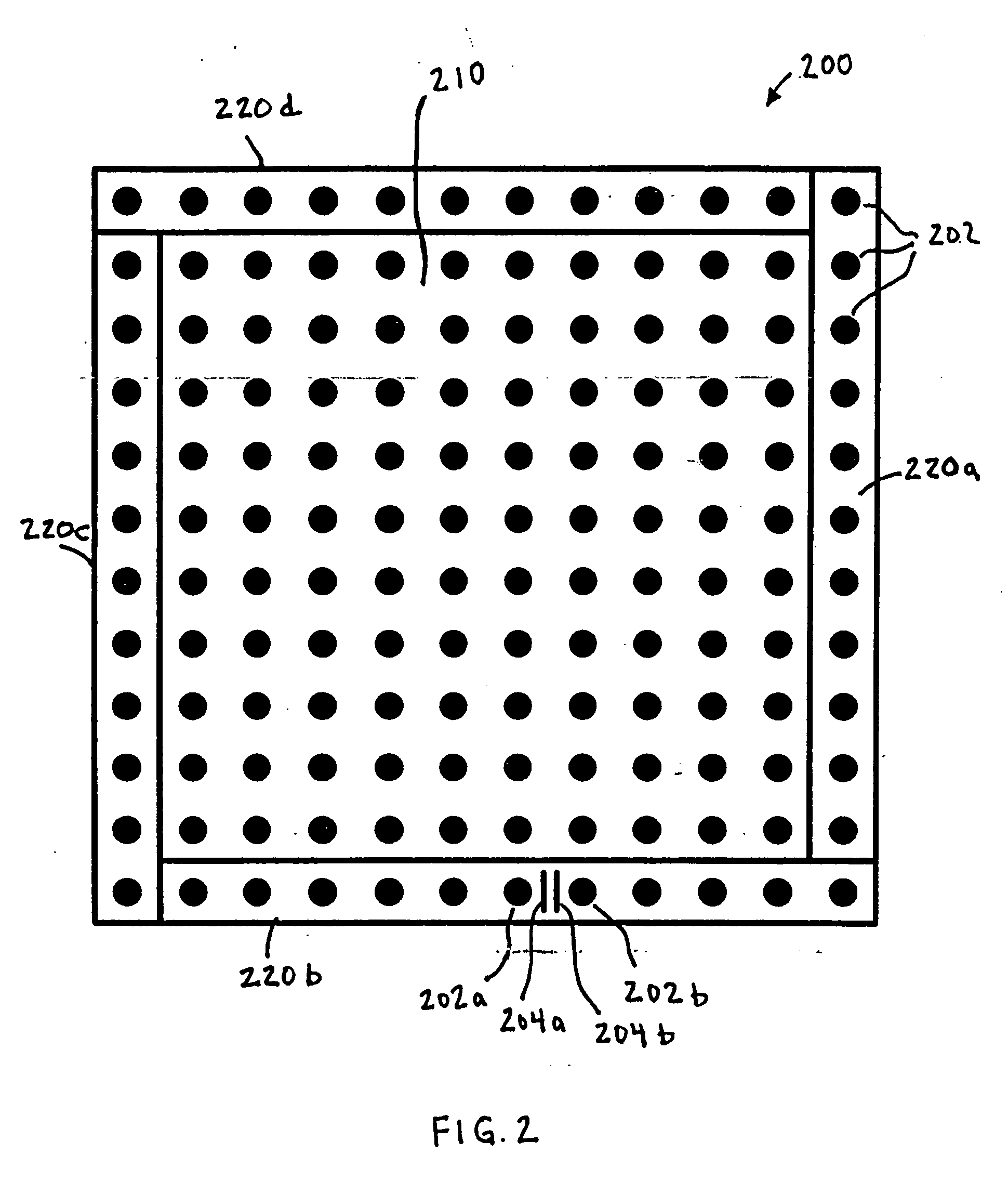
The present invention is directed to the optimization of routing layers and board space requirements in integrated circuit (IC) packages and printed circuit boards (PCBs). For example, the present invention is applicable in land grid array (LGA), pin grid array (PGA), chip scale package (CSP), ball grid array (BGA), and other integrated circuit package types, and their respective PCB land patterns. The present invention is applicable to all types of package substrates, including ceramic, plastic, and tape (flex) substrates. Furthermore the present invention is applicable to die-up (cavity-up) and die-down (cavity-down) IC die orientations. For illustrative purposes, the present invention is described herein as being implemented in a BGA package. However, the present invention is applicable to the other integrated circuit package types mentioned herein, and to additional integrated circuit package types.

Note that the terms “contact pad,”“contact,” and “conductive pad” ar...


PUM


Abstract

A method and apparatus for improved contact pad arrays and land patterns for integrated circuit packages are presented. A plurality of conductive pads are arranged in an array of rows and columns. At least one edge of a perimeter of the array is not fully populated with conductive pads. Spaces created in the edge by missing conductive pads create additional routing channels for signals from conductive pads within the array to be routed external to the array through the edge. A land pattern may have routing channels on one or more layers of a printed circuit board. In such a multi-layer land pattern, spaces can be created in edges on any number of the layers. Furthermore, corner pad arrangements having known routing channel characteristics can be used in any number of corners of a land pattern that incorporates spaces in an edge.

Description

BACKGROUND OF THE INVENTION 1. Field of the Invention The present invention relates to integrated circuit packaging, and more particularly, to improved routing in integrated circuit packages and in circuit boards to which they are mounted. 2. Background Art Integrated circuit (IC) dies are typically mounted in or on a package that is attached to a printed circuit board (PCB). One such type of IC die package is a ball grid array (BGA) package. BGA packages provide for smaller footprints than many other package solutions available today. A BGA package has an array of solder ball pads located on a bottom external surface of a package substrate. Solder balls are attached to the solder ball pads. The solder balls are reflowed to attach the package to the PCB. The IC die is mounted to a top surface of the package substrate. Wire bonds typically couple signals of the IC die to the substrate. The substrate has internal routing which electrically couples the IC die signals to the solder ...

Claims


Application Information

Patent Timeline
Patent Type & Authority Applications(United States)
IPC IPC(8): H01L23/498H01L23/50H05K1/11H05K3/00
CPCH01L23/49816H01L23/49838H01L23/50H01L2224/48227H01L2924/15173H01L2924/01019H05K1/112H05K3/0005H05K2201/09227H05K2201/10734H01L24/48H01L2924/15311H01L2224/05599H01L2224/45099H01L2224/85399H01L2924/00014H01L2924/14H01L2924/181H01L2924/00012H01L2224/45015H01L2924/207H01L2924/00
Inventor SEAMAN, KEVIN L.WNEK, VERNON M.
Owner AVAGO TECH INT SALES PTE LTD
Why Eureka
Try Eureka