

Method for manufacturing stamper, stamper and optical recording medium
a manufacturing method and stamping technology, applied in the field of manufacturing stamping devices, can solve problems such as environmental problems, and achieve the effect of reducing defects in the mother stamping devi
- Summary
- Abstract
- Description
- Claims
- Application Information
AI Technical Summary
Benefits of technology
Problems solved by technology
Method used
Image

Examples
example 1
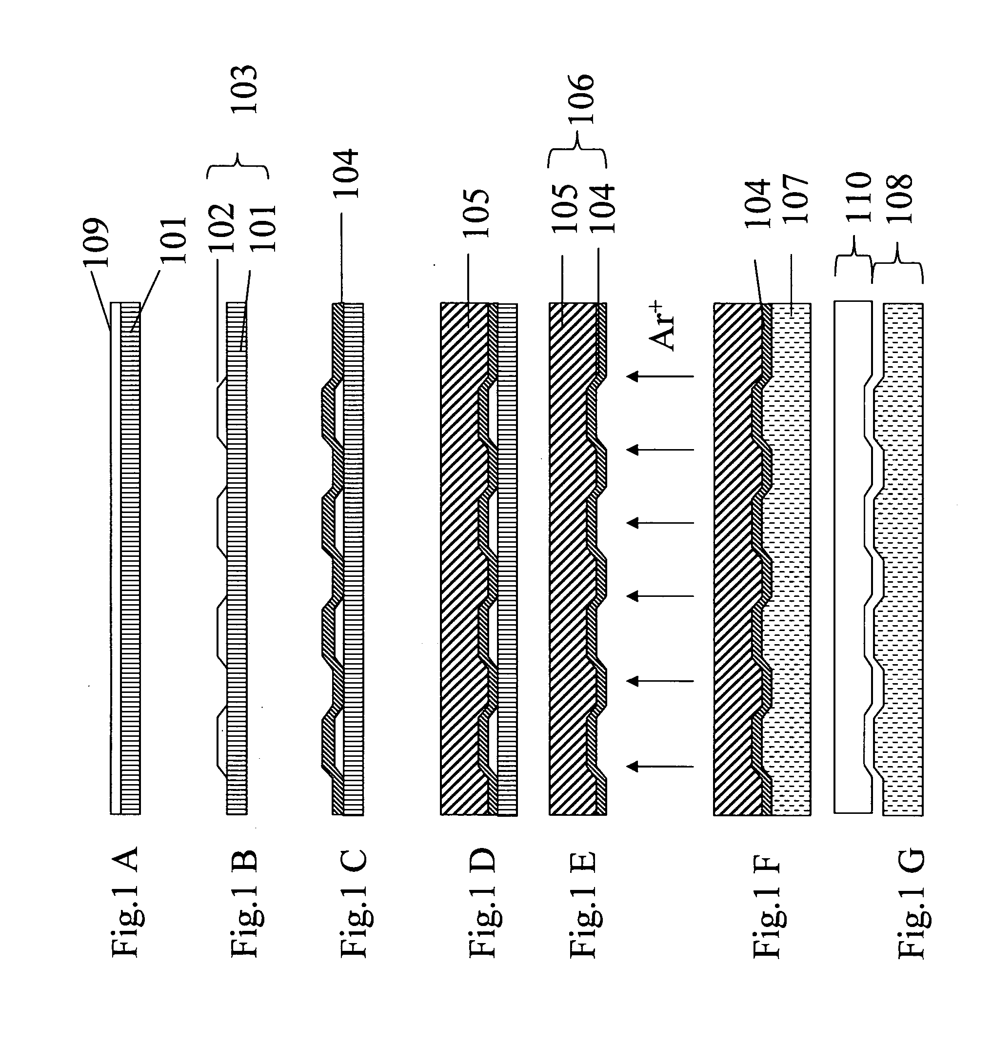
[0051] (1)
[0052] Experiments used to ascertain the etching conditions will be described with regard to examination of the dependence of input power during etching. Note that because time dependence during the etching is not important, it is assumed to be constant at 90 seconds.
[0053] The results are shown in Table 1.
TABLE 1Input Power of theNoiseEtching (W)Separability(dBm)10BadN / A30BadN / A50Good−71200Good−73500Good−72600Good−68800Good−651000Good−58
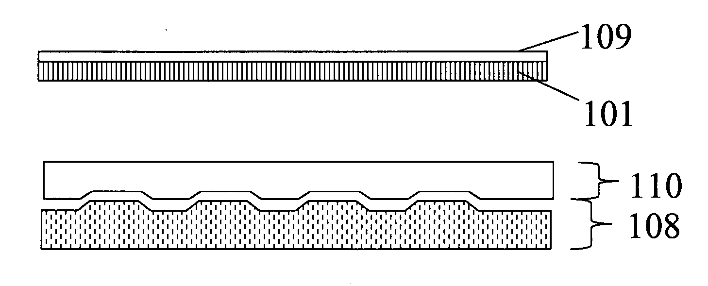
[0054] In Table 1, the term “Bad” in the separability column indicates etching conditions in which the electroformed film (II) 107 could not be separated from the father stamper 106, or conditions in which defects were produced on the electroformed film (II) 107. The term “Good” in the same column indicates conditions in which a mother stamper 108 without defects was produced.
[0055] In addition, the mother stamper 108 is set on an injection molding machine, and then a substrate for an optical recording medium with a thickness of 1.1 m...
example 2
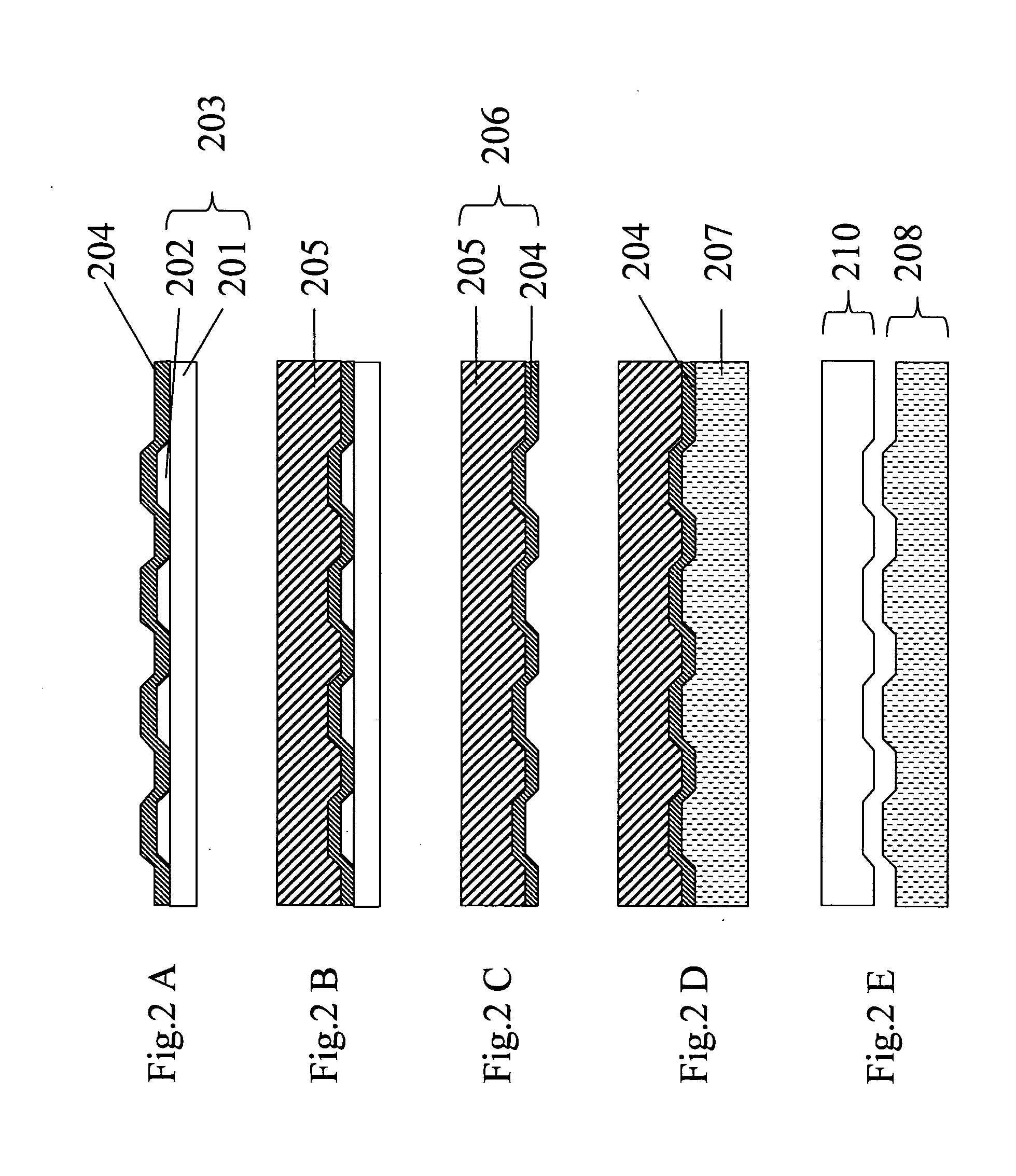
[0059] (1)
[0060] In Example 2, a mother stamper 108 will be formed via the same steps and procedures as described above. FIG. 1 will be used to describe this.
[0061] It is thought that there is a relationship between the separability of the mother stamper 108 and the existence of defects on the stamper and whether it is possible to form nickel hydroxide uniformly on the father stamper 106. To form the hydroxide uniformly on the stamper, the stamper needs to be immersed in water quickly after the plasma surface treatment. On the contrary, after the treatment, if the father stamper 106 is left in the atmosphere, both nickel oxide and nickel hydroxide are produced. Because the ratios of nickel oxide to nickel hydroxide are different locally, and the separabilities of these materials are also different, then the difference of the separability may occur locally and the possibility of defects remaining on the mother stamper 108 increases.
[0062] In Table 3, the relationship between the t...
PUM
| Property | Measurement | Unit |
|---|---|---|
| electric power | aaaaa | aaaaa |
| electric power | aaaaa | aaaaa |
| contact angle | aaaaa | aaaaa |
Abstract
Description
Claims
Application Information