
Method for producing a master disk of a recording medium, method for producing a stamper, method for producing a recording medium, master disk of a recording medium, stamper of a recording medium, and recording medium
- Summary
- Abstract
- Description
- Claims
- Application Information
AI Technical Summary
Benefits of technology
Problems solved by technology
Method used
Image

Examples
embodiment 1
[0047] (Embodiment 1)
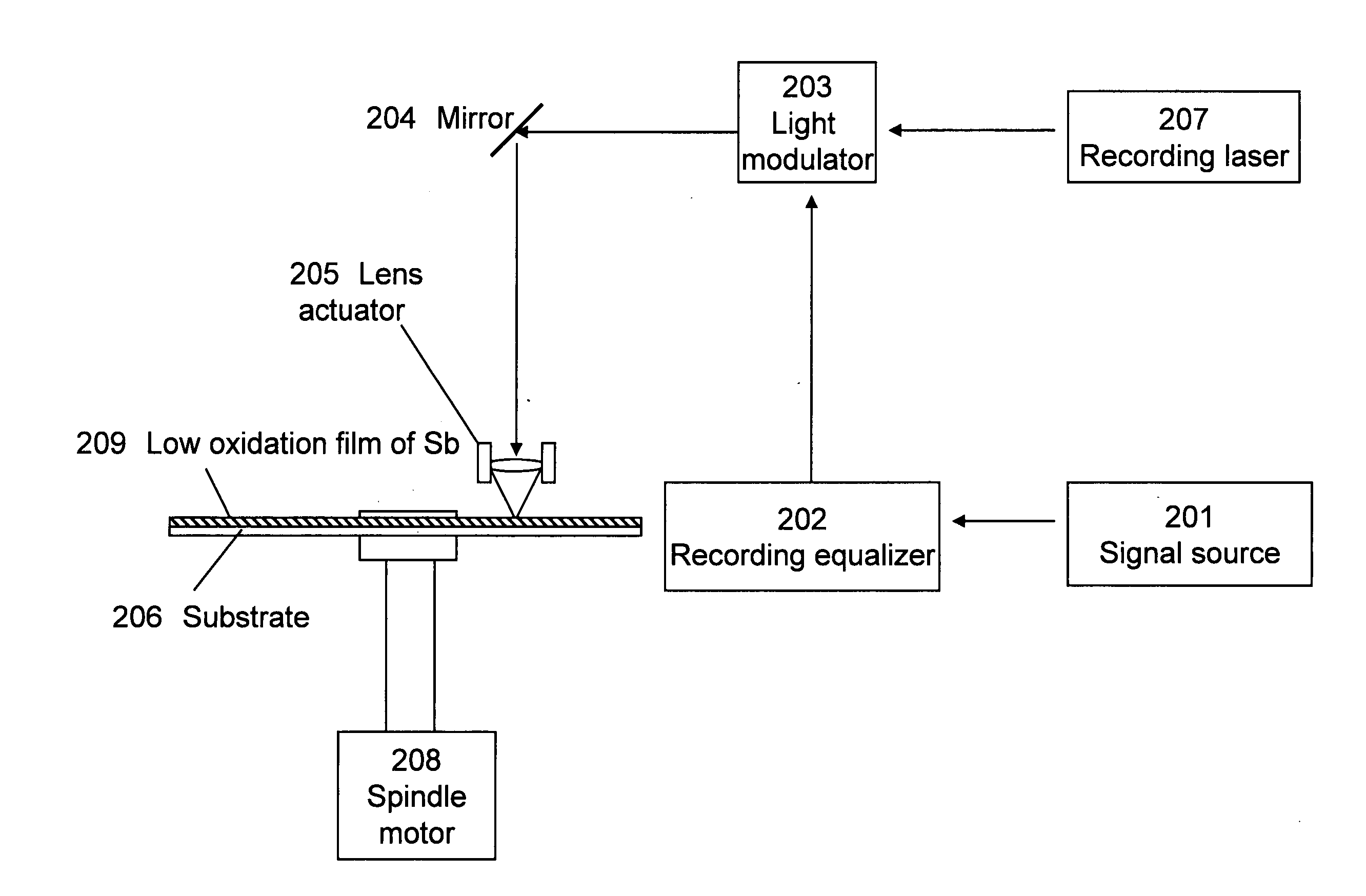
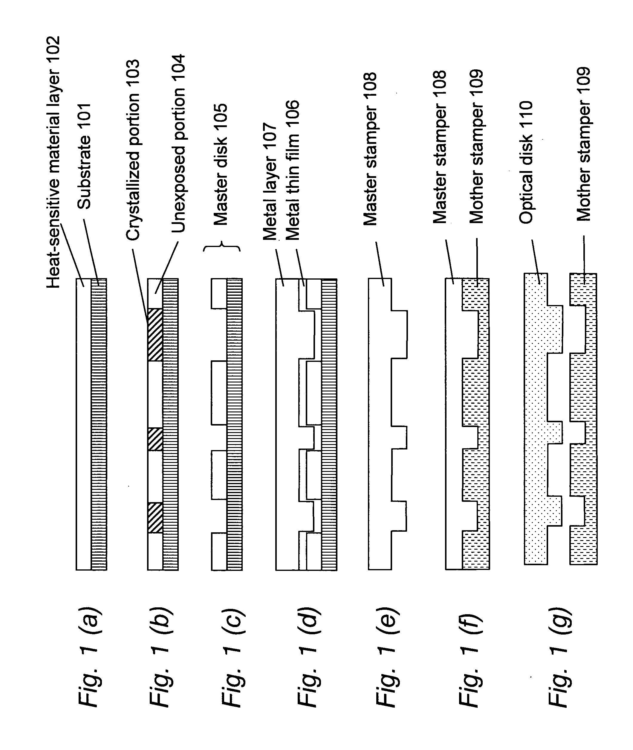
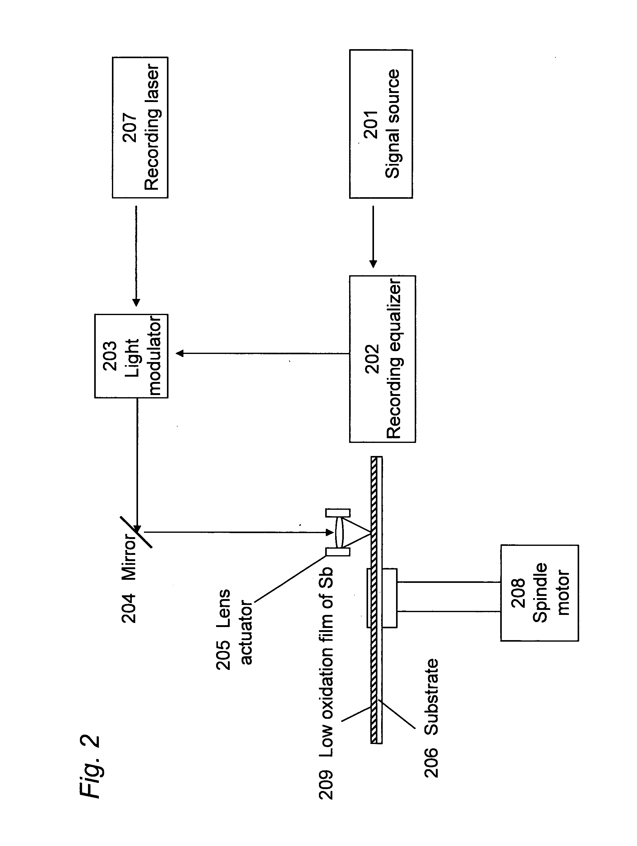
[0048] In Embodiment 1, a low oxidation film was formed as a heat-sensitive material layer 102 on a substrate 101 such as an abraded glass substrate. After a direct current magnetron sputtering apparatus was equipped with a Sb target and after the glass substrate 101 was fixed on a substrate holder, the inside of the chamber was vacuum discharged using a cryopump up to a high vacuum of 1×10⁻⁴ Pa. While vacuum discharging, Ar gas was introduced into the chamber up to 0.10 Pa and then an O2 gas was introduced up to a total pressure of 0.11 Pa. Thereafter, while rotating the substrate 101, direct current was applied to the Sb target to form the film such that the film thickness of the Sb oxide became 80 nm.
[0049] In the present embodiment, by introducing an O2 gas during film formation, a low oxidation Sb film could be formed on the substrate 101. However, a material with a composition of a low oxidation Sb film may be used for the target material to perform sputt...
embodiment 2
[0058] (Embodiment 2)
[0059] In Embodiment 2, film formation, recording and development were performed in the same manner as that of Embodiment 1. In the present embodiment, when Sb is film-formed as a heat-sensitive material under an atmosphere of O2, a target of Te using as an additive was electrically discharged at the same time to form a low oxidation film of Sb and Te. The Te content was adjusted by altering the input power of Te during sputtering.
[0060] Addition of Te to a heat-sensitive material layer 102 that contains Sb as the main component enabled a reduction in surface roughness of unexposed portion 104 during development. This surface roughness of the unexposed portion 104 is thought to be attributable to low resistance to a development fluid of portions incapable of maintaining a stable amorphous state. In Embodiment 2, it is thought that by addition of Te, the solubility of which is smaller than the solubility of Sb2O3, the Te can be separated out on the film surface ...
embodiment 3
[0064] (Embodiment 3)
[0065] The present embodiment will be set forth referring to FIG. 3. In the same manner as that of Embodiment 1, a low oxidation Sb film as a heat-sensitive material layer 302 was formed on a substrate 301 comprising Si by means of the magnetron sputtering process (FIG. 3(a)). Thereafter, to prevent the occurrence of defects in unexposed portions from the developing treatment, the heat-sensitive material layer 302 was subjected to an annealing treatment (FIG. 3(b)). The annealing treatment here was performed by placing the substrate 301 on which the heat-sensitive material layer 302 was formed in a clean oven. By measuring the temperature of the heat-sensitive material layer 302 and using the same recording apparatus as in Embodiment 1, minute crystallized portions were formed in the heat-sensitive material layer 302 (FIG. 3(c)). Subsequently, the crystallized portions were removed by soaking the resultant material in a 2% aqueous tetramethylammonium hydroxide s...
PUM
| Property | Measurement | Unit |
|---|---|---|
| Temperature | aaaaa | aaaaa |
| Temperature | aaaaa | aaaaa |
| Partial pressure | aaaaa | aaaaa |
Abstract
Description
Claims
Application Information