
IC card

a technology of ic cards and integrated circuits, applied in the field of ic cards, can solve the problems of difficult mounting of much more integrated circuits, limitation of the size of the holding of the ic chip, and inability to memorize the data of the ic card, and achieve the effect of reducing cost and high function

Inactive Publication Date: 2005-03-03
SEMICON ENERGY LAB CO LTD
View PDF80 Cites 144 Cited by
  • Summary
  • Abstract
  • Description
  • Claims
  • Application Information

AI Technical Summary

Benefits of technology

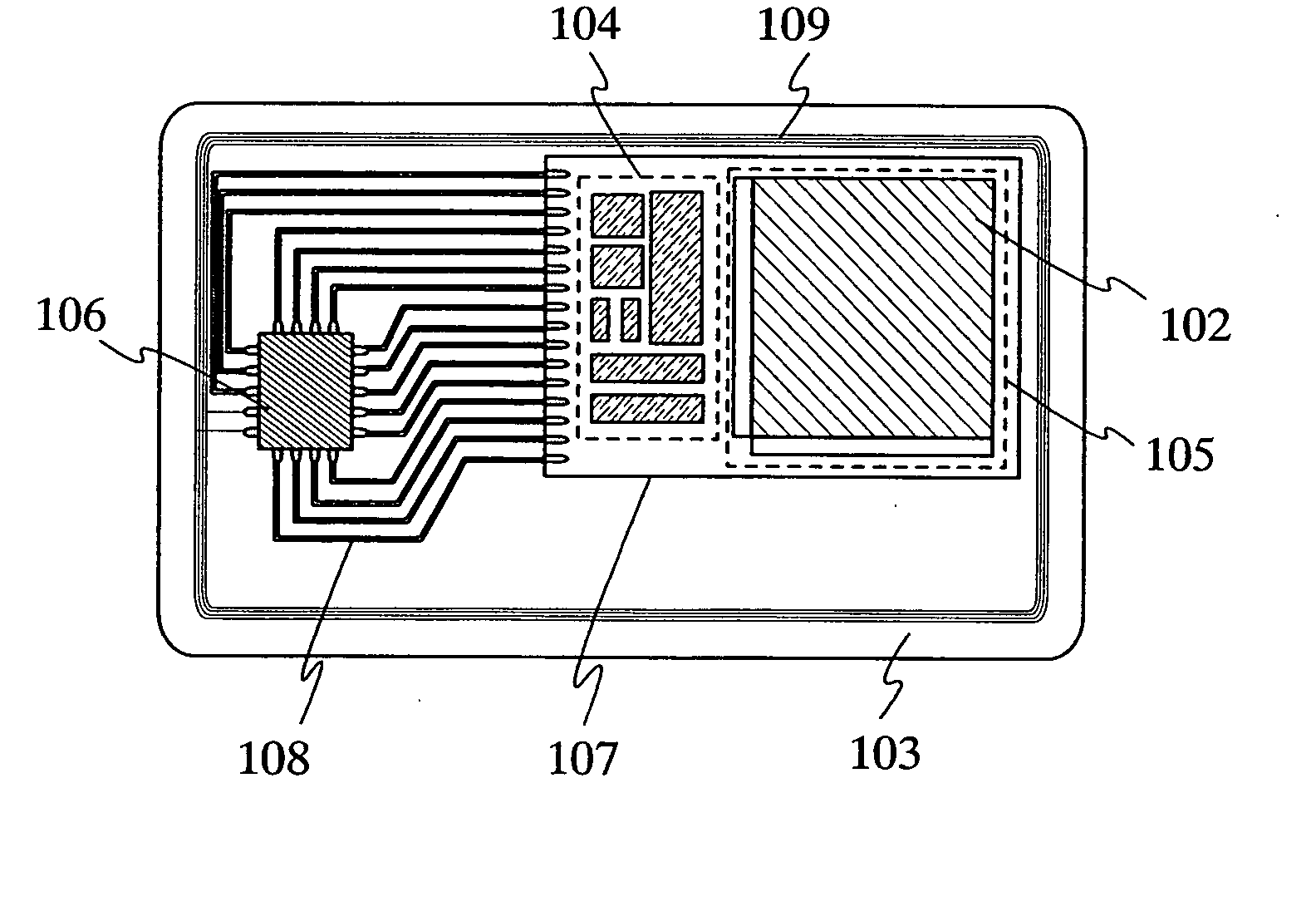
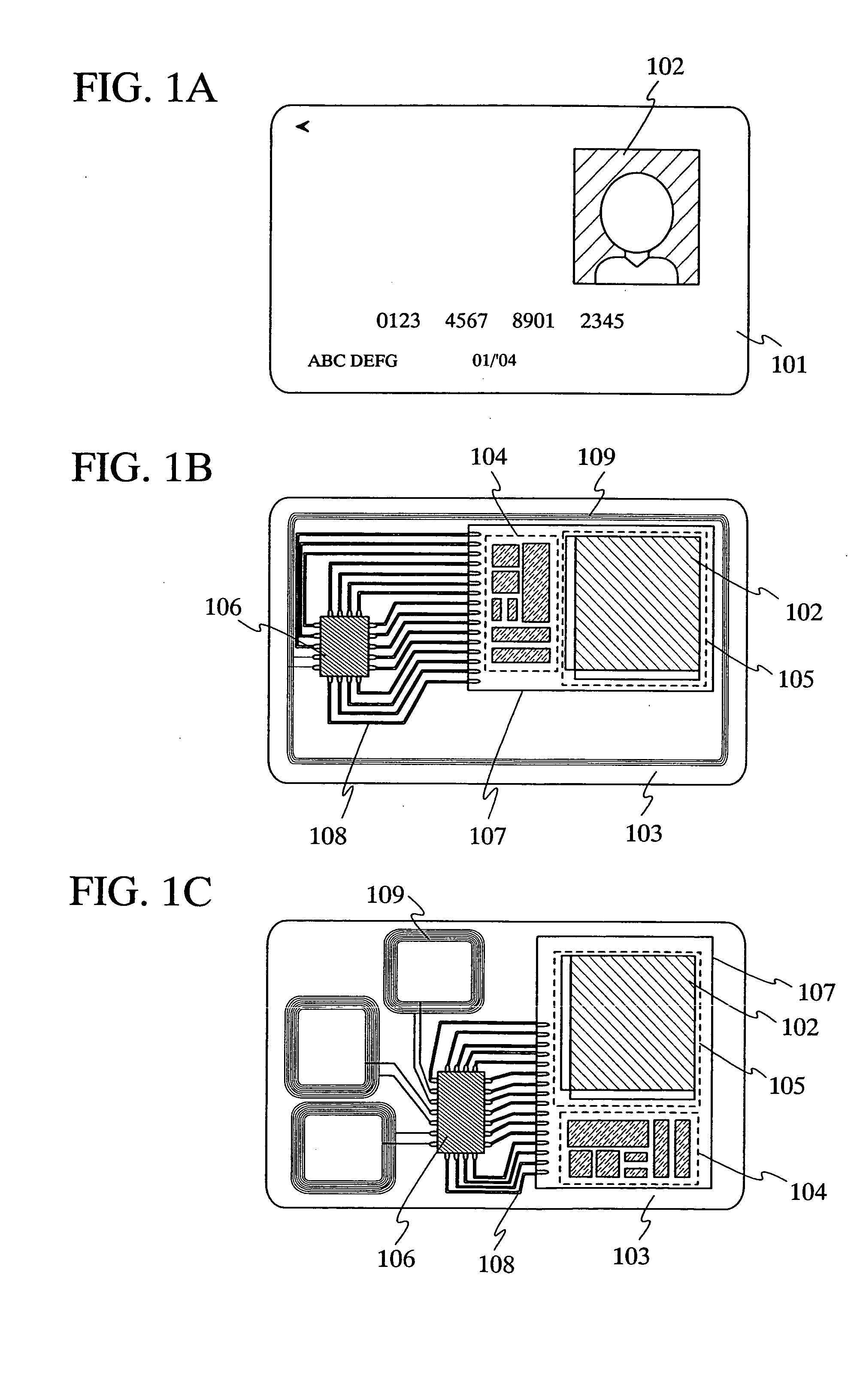
[0012] It is an object of the present invention to provide an IC card that can realize high function without increasing the size of an IC chip, and that can realize cost reduction. Further, it is another object of the present invention to provide an IC card that can ensure security by preventing forgery such as changing a picture of a face, and that can display other images as well as a picture of a face.
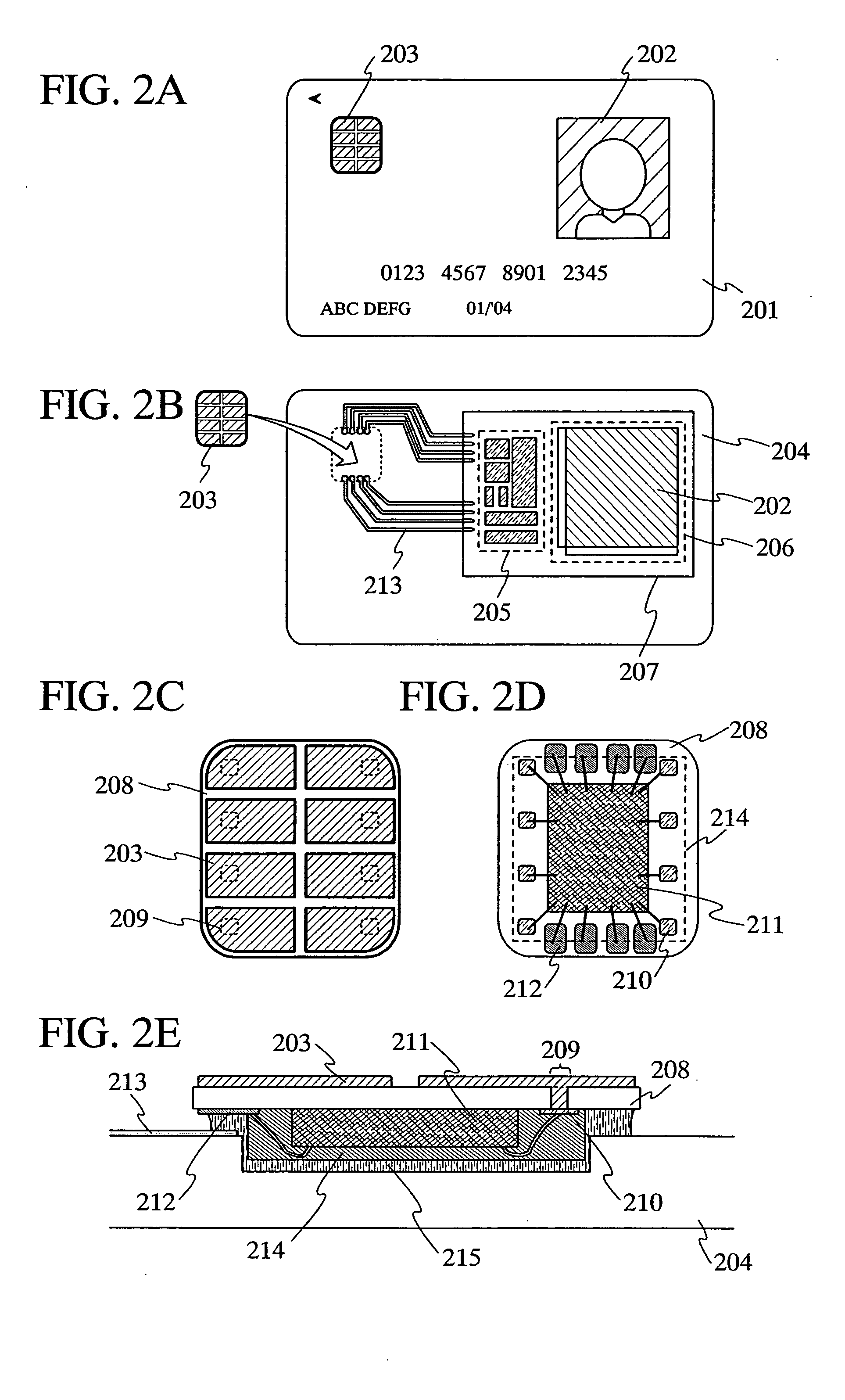
[0015] Note that an integrated circuit formed on an IC chip can be operated with higher frequency and has a smaller variation on characteristics of a semiconductor element than a thin film integrated circuit. Therefore, it is preferable that a radio frequency (RF) circuit in which an operation at high frequency is required or an analog circuit which is easy to be affected by a variation of characteristics of a semiconductor element is formed in an IC chip. A digital circuit that is less affected by a variation of characteristics of a semiconductor element than an analog circuit or a low operation frequency circuit that can operate favorably with a thin semiconductor element or the like is preferably mounted on an IC card as a thin film integrated circuit. When a memory having a larger capacity is required, a memory may be formed on an IC chip. A memory may be formed as a thin film integrated circuit if the capacity of a memory can be controlled. As mentioned above, the yield of the whole integrated circuit can be increased and cost can be reduced by forming individually a circuit to be mounted as an IC chip and a circuit to be mounted as a thin film integrated circuit depending on characteristics of the circuits. A higher function IC card can be obtained while downsizing an IC chip.
[0018] Moreover, a thin film integrated circuit that has been formed separately may be attached and laminated to increase a circuit scale or a memory capacity. A thin film integrated circuit is much thinner than an IC chip formed by using a semiconductor substrate, and thus, the mechanical intensity of an IC card can be maintained to some extent even when plural thin film integrated circuits are laminated. A connection between the laminated thin film integrated circuits can be made by using a known connection method such as a flip chip method, a TAB (Tape Automated Bonding) method, or a wire bonding method.
[0020] In the present invention, because not only an IC chip but also a thin film integrated circuit of 5 μm thick in total, preferably about 2 μm, is mounted on an IC card, a circuit scale or a memory capacity of the whole integrated circuit can be increased and a higher function IC card can be obtained while downsizing an IC chip. The thickness of a display device can be set to about 0.5 mm, preferably, about 0.3 mm. Accordingly, it is possible to provide a display device for an IC card having a thickness of from 0.5 mm through 1.5 mm. A large scale integrated circuit is formed by combining a thin film integrated circuit and an IC chip that are each formed separately, and therefore, the yield can be more increased than the case of forming integrated circuits on one substrate simultaneously.

Problems solved by technology

Further, the IC card has merits that the IC card does not have a risk that data is read out by a physical means such as putting iron sand on the card, different from a magnetic card, and that data memorized in the IC card is not easily falsified.
Therefore, there is naturally a limitation on the size of an IC chip in holding the intensity for bending of an IC card to some extent.
Accordingly, it is difficult to mount much more integrated circuits that are larger in a circuit scale or a memory capacity, on an IC chip having a limitation on its size, thereby preventing the integrated circuits from having higher functions.
As an IC card is used more widely, a misapplication of an IC card becomes a bigger problem measurably.
A future issue is how securely identification is performed when an IC card is used.
However, in general, a picture of a face is transferred on an IC card by a printing method, and thus there is a pitfall that the picture of the face is easily changed by forgery.

Method used


Image

  • IC card
  • IC card
  • IC card

Examples


embodiment 1

[0108] A method for manufacturing a thin film integrated circuit and a display device is described. Note that, in this embodiment, although a TFT is given as an example of a semiconductor element, the semiconductor element included in the thin film integrated circuit and the display device is not limited thereto, and various circuit elements can be used. For example, a memory element, a diode, a photoelectric transferring element, a resistor element, a coil, a capacitor element, an inductor and the like can be given as a representative example in addition to a TFT.

[0109] As shown in FIG. 9A, a metal film 501 is formed on a first substrate 500 by sputtering. The metal film 501 is made of tungsten to be from 10 nm to 200 nm, preferably from 50 nm to 75 nm in thickness. In this embodiment, the metal film 501 is formed directly on the first substrate 500. However, the first substrate 500 may be covered with an insulating film such as a silicon oxide, a silicon nitride, a silicon oxynit...

embodiment 2

[0151] Next, an example of manufacturing a plurality of IC cards using a large-size substrate is described. FIG. 14A shows a state in which a display device, an antenna coil, and a thin film integrated circuit corresponding to a plurality of IC cards are formed over a large-size card substrate 601. FIG. 14A shows a state before a covering material is bonded by resin after a protective layer is removed. A region 602 surrounded by a dotted line corresponds to one IC card. In the case of using a liquid crystal display device as a display device, a liquid crystal may be injected by a dispenser method or a dip method. However, the dispenser method is employed when an injection port for a liquid crystal for the dip method cannot be arranged in an edge portion of a card substrate, as shown in FIG. 14A.

[0152] An IC chip 606 corresponding to each IC card is mounted, as shown in FIG. 14B.

[0153] Resin 603 is applied to cover the IC chip 606, the thin film integrated circuit, the display devi...

embodiment 3

[0156] A liquid crystal material suitable for the case where a liquid crystal display device is used as a display device and the case where a display element is transferred after completed, is described in this embodiment.

[0157]FIGS. 15A and 15B are cross sectional views of a liquid crystal display device of this embodiment. A columnar spacer 1401 is provided for a pixel in a liquid crystal display device shown in FIG. 15A. The adhesion between an opposite substrate 1402 and a substrate 1403 on the side of elements is enhanced by the columnar spacer 1401. This makes it possible to prevent a semiconductor element in the outside of the area overlapping with a sealing material from remaining on the side of the first substrate, when the first substrate is separated.

[0158]FIG. 15B is a cross sectional view of a liquid crystal display device using a nematic liquid crystal, a smectic liquid crystal, a ferroelectric liquid crystal, or a PDLC (polymer dispersed liquid crystal) containing t...


PUM


Abstract

The present invention provides an IC card that can realize high function without increasing the size of an IC chip, and that can realize cost reduction. The IC card comprises a first single crystal integrated circuit, a second integrated circuit, and a display device. The second integrated circuit and the display device are each formed from a thin film semiconductor film, over a plastic substrate, and the first single crystal integrated circuit is mounted on the plastic substrate so as to be electrically connected to the second integrated circuit.

Description

BACKGROUND OF THE INVENTION [0001] 1. Field of the Invention [0002] The present invention relates to an IC card (which is also called a smart card) incorporating an integrated circuit such as a memory or a microprocessor (CPU), and a display device that can display an image. [0003] 2. Description of the Related Art [0004] Several ten bytes of data only can be memorized in a magnetic card that can memorize data magnetically. However, an IC card (an electronic card) incorporating a semiconductor memory, normally, can memorize about 5 KB of data or more. The IC card can assure much more capacity than a magnetic card. Further, the IC card has merits that the IC card does not have a risk that data is read out by a physical means such as putting iron sand on the card, different from a magnetic card, and that data memorized in the IC card is not easily falsified. [0005] It is noted that a category of a card typified by an electronic card includes an ID card to serve as an identification pa...

Claims


Application Information

Patent Timeline
IPC IPC(8): G06K19/07G06K19/077H01L23/538
CPCG06K19/0704G06K19/072H01L2924/01047H01L2924/01015H01L2924/10253H01L24/48H01L2224/45147H01L2924/3025H01L2924/19041H01L2924/12044H01L2924/01079G06K19/0723G06K19/077G06K19/07703G06K19/07743G06K19/07747G06K19/07749H01L23/5388H01L2224/16H01L2224/48091H01L2224/48227H01L2924/00014H01L2924/00H01L2924/12042H01L24/45H01L2924/14H01L2224/05599
Inventor YAMAZAKI, SHUNPEI
Owner SEMICON ENERGY LAB CO LTD
Learn More