Chip stack package and manufacturing method thereof

a technology of chip stacking and manufacturing method, applied in the field of three-dimensional multi-chip stack package, can solve the problems of increasing the manufacturing time and cost associated with stacking individual chips, increasing the manufacturing cost associated with wafer-level chip stacking process, and increasing the chip size of advanced devices. achieve the effect of reducing manufacturing time, manufacturing cost and yield loss

Active Publication Date: 2005-03-03
SAMSUNG ELECTRONICS CO LTD
View PDF10 Cites 506 Cited by
  • Summary
  • Abstract
  • Description
  • Claims
  • Application Information

AI Technical Summary

Benefits of technology

[0010] The exemplary embodiments of the present invention provide a variety of chip stack packages and methods for man

Problems solved by technology

With the rapid advancement of very large scale integrated circuit (VLSI) technologies, traditional packaging is becoming a performance bottleneck of the advanced microelectronics devices.
Furthermore, the chip size of the advanced devices continues to grow although sub-micron processing technologies continue to reduce the minimum feature sizes on the devices.
Relative to single chip packaging, however, such conventional multi-chip stack packaging methods, however, tend to incur increased manufacturing time and cost associated with stacking the individual chips.
Unfortunately, wafer

Method used


Image

  • Chip stack package and manufacturing method thereof
  • Chip stack package and manufacturing method thereof
  • Chip stack package and manufacturing method thereof

Examples


Embodiment Construction

[0025] The present invention will now be described more fully hereinafter with reference to the accompanying drawings, in which several exemplary embodiments of the invention are illustrated. This invention may, however, be embodied in many different forms and should not be construed as limited to the particular embodiments set forth herein. Rather, these embodiments are provided so that this disclosure will be thorough and complete, and will fully convey the scope of the invention to those skilled in the art.

[0026] In the description, well-known structures and processes have not been described or illustrated in detail to avoid obscuring the present invention. It will be appreciated that for simplicity and clarity of illustration, some elements illustrated in the figures have not necessarily been drawn to scale. For example, the dimensions of some of the elements have been exaggerated or reduced relative to other elements for clarity.

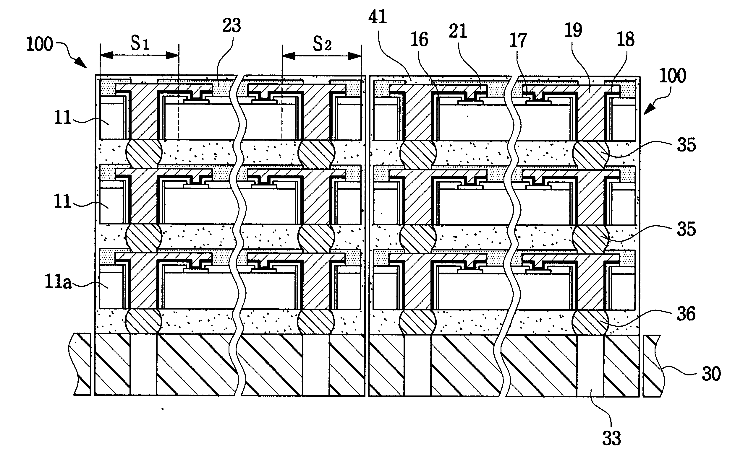
[0027] As illustrated in FIG. 3 a chip stack pa...


PUM


Abstract

A chip stack package is manufactured at a wafer level by forming connection vias in the scribe lanes adjacent the chips and connecting the device chip pads to the connection vias using rerouting lines. A lower chip is then attached and connected to a substrate, which may be a test wafer, and an upper chip is attached and connected to the lower chip, the electrical connections being achieved through their respective connection vias. In addition to the connection vias, the chip stack package may include connection bumps formed between vertically adjacent chips and/or the lower chip and the substrate. The preferred substrate is a test wafer that allows the attached chips to be tested, and replaced if faulty, thereby ensuring that each layer of stacked chips includes only “known-good die” before the next layer of chips is attached thereby increasing the production rate and improving the yield.

Description

CROSS REFERENCE TO RELATED APPLICATIONS [0001] This U.S. non-provisional application claims priority under 35 U.S.C. § 119 to Korean Patent Application No. 2003-59166, filed Aug. 26, 2003, the contents of which are incorporated by reference.BACKGROUND OF THE INVENTION [0002] 1. Field of the Invention [0003] The present invention relates generally to electronic packaging technology and, more particularly, to a three-dimensional multi-chip stack package and a method for manufacturing such chip stack packages. [0004] 2. Description of the Related Art [0005] With the rapid advancement of very large scale integrated circuit (VLSI) technologies, traditional packaging is becoming a performance bottleneck of the advanced microelectronics devices. This is due to the rapidly increasing of pin count and clock speed on the advanced devices. Along with the fast clock speed, power distribution of the advanced devices also is an important issue that must be addressed. Furthermore, the chip size of...

Claims


Application Information

Patent Timeline
IPC IPC(8): H01L23/52H01L21/3205H01L21/768H01L21/98H01L23/48H01L25/065H01L25/07H01L25/18
CPCH01L21/76898H01L23/481H01L23/5389H01L24/24H01L24/82H01L24/97H01L25/0657H01L25/50H01L2224/16145H01L2224/24226H01L2224/32145H01L2224/48091H01L2224/48095H01L2224/48227H01L2224/73265H01L2224/97H01L2225/06513H01L2225/06541H01L2225/06586H01L2924/01013H01L2924/01029H01L2924/01074H01L2924/01078H01L2924/01079H01L2924/04941H01L2924/14H01L2924/15311H01L2924/18162H01L24/48H01L2924/01006H01L2924/01033H01L2924/014H01L2224/32225Y10S438/977H01L2224/16225Y10T436/108331Y10T436/104998Y10T436/17Y10T436/175383H01L2924/00014H01L2224/81H01L2224/82H01L2924/00H01L24/02H01L24/03H01L24/05H01L24/11H01L24/16H01L24/81H01L2224/02372H01L2224/02379H01L2224/05001H01L2224/05008H01L2224/05022H01L2224/05024H01L2224/05124H01L2224/05166H01L2224/05548H01L2224/05556H01L2224/05569H01L2224/06181H01L2224/13009H01L2224/13025H01L2224/16146H01L2224/16235H01L2224/17181H01L2924/0001H01L2924/12042H01L2924/181Y02P80/30H01L2224/05599H01L2924/00012H01L2224/45099H01L2224/45015H01L2924/207H01L2224/02H01L23/48
Inventor LEE, KANG-WOOKKIM, GU-SUNGJANG, DONG-HYEONBAEK, SEUNG-DUKCHUNG, JAE-SIK
Owner SAMSUNG ELECTRONICS CO LTD
Why Eureka
Try Eureka