

Microbeam assembly and associated method for integrated circuit interconnection to substrates
- Summary
- Abstract
- Description
- Claims
- Application Information
AI Technical Summary
Benefits of technology
Problems solved by technology
Method used
Image

Examples
Embodiment Construction
[0026] The present invention will now be described more fully with reference to the accompanying drawings, in which preferred embodiments of the invention are shown. This invention may, however, be embodied in many different forms and should not be construed as limited to the embodiments set forth here; rather, these embodiments are provided so that this disclosure will be thorough and complete and will fully convey the scope of the invention to those skilled in the art. Like numbers refer to like elements throughout.
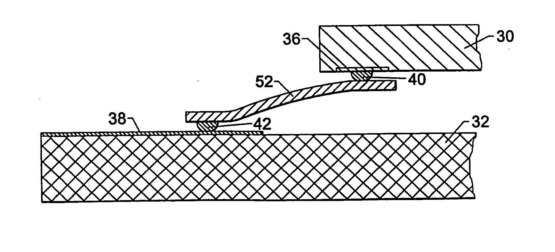
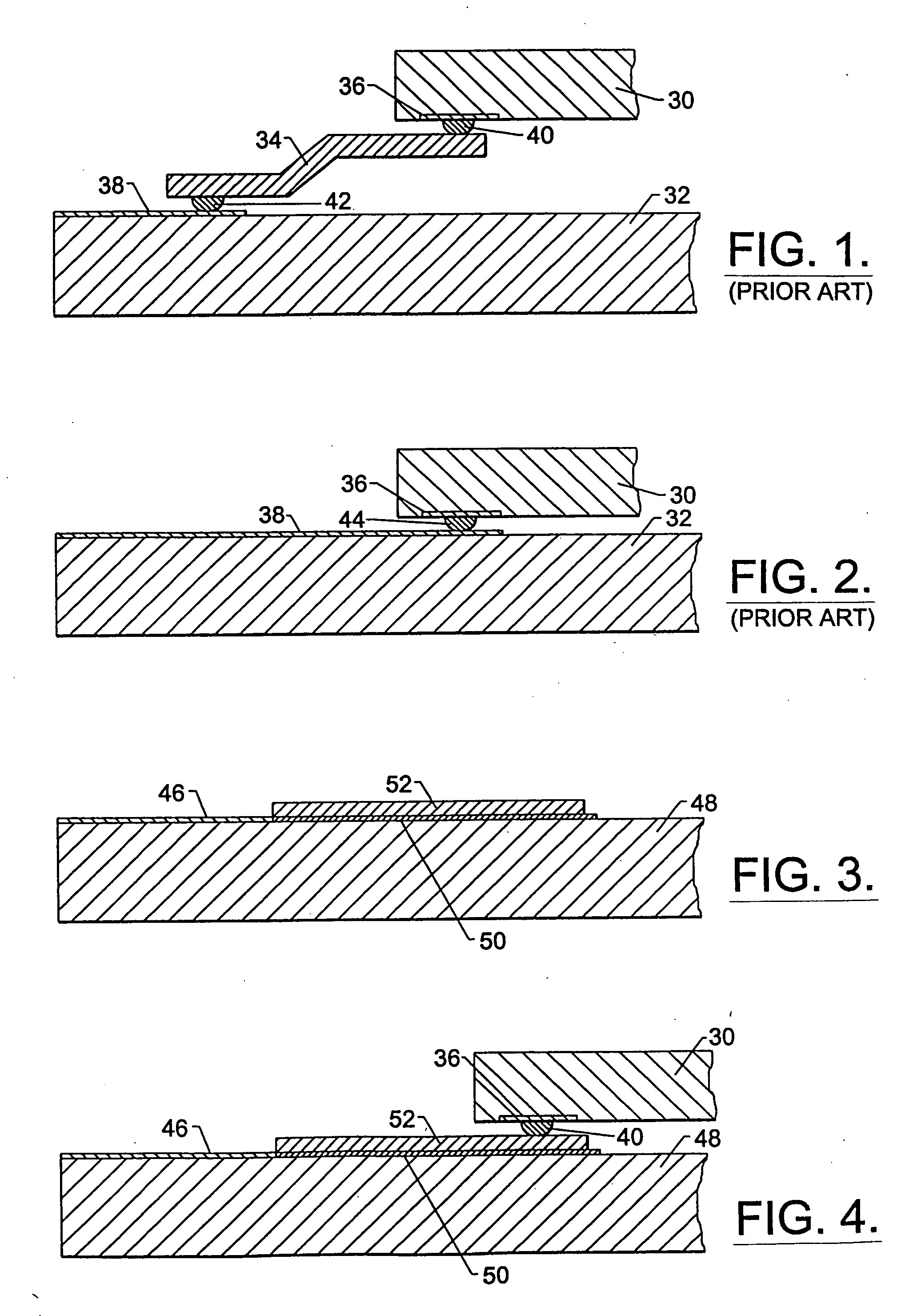
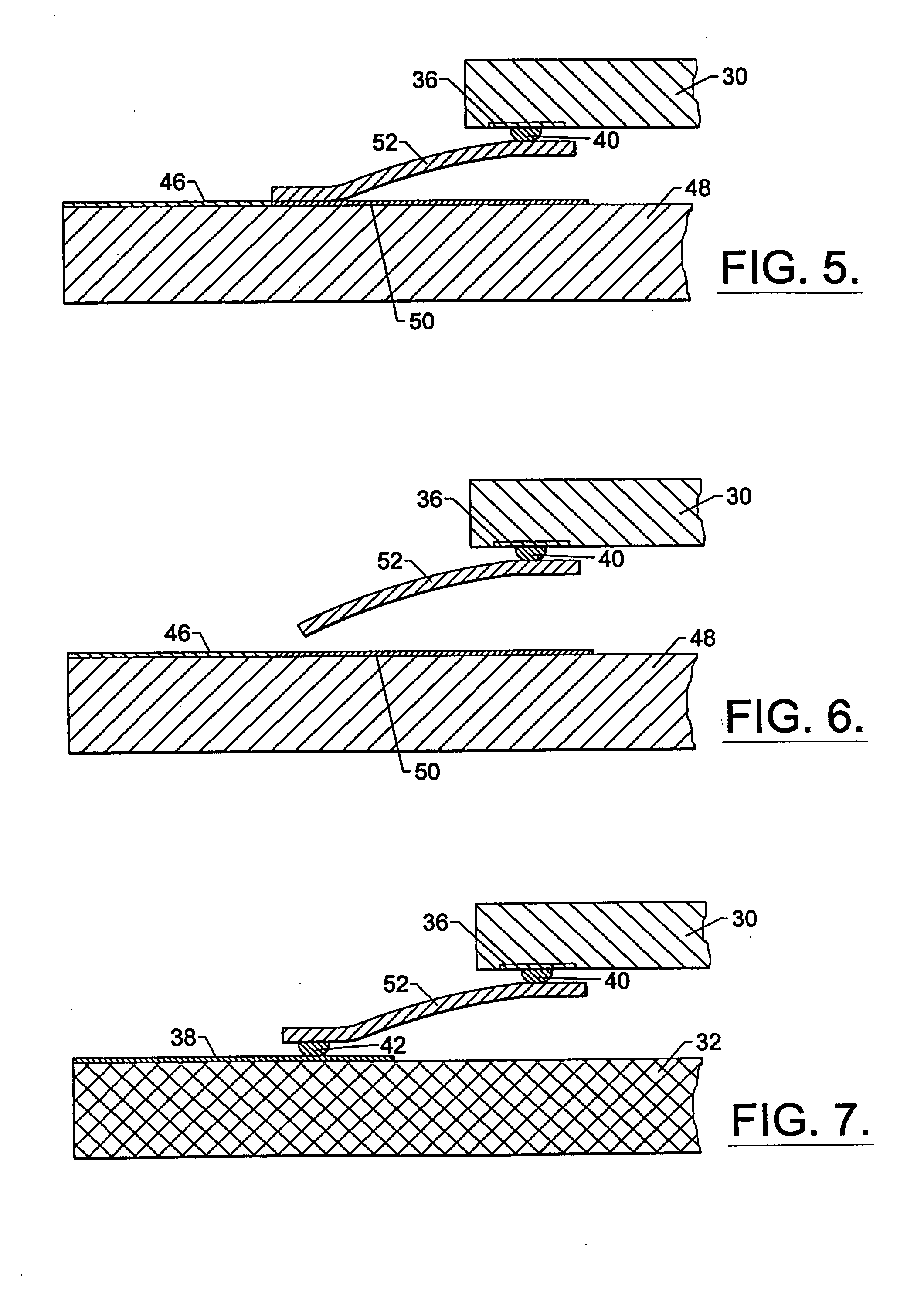
[0027] One advantageous embodiment of the microbeam assembly according to the present invention is depicted in FIG. 3. In FIG. 3, fan-out conductors 46 have been patterned on portions of a carrier 48 and a release layer 50 has been deposited on the carrier 48 on areas adjacent the fan-out conductors 46. The release layer 50 may be a thin layer of tungsten or other suitable material which may be deposited on a carrier to allow a conductive microbeam 52 to be formed via ...
PUM
| Property | Measurement | Unit |
|---|---|---|
| Force | aaaaa | aaaaa |
| Electrical conductor | aaaaa | aaaaa |
Abstract
Description
Claims
Application Information