High isolation/high speed buffer amplifier

a buffer amplifier and high isolation technology, applied in the direction of amplifiers, dc-amplifiers with dc-coupled stages, single-ended push-pull amplifiers, etc., can solve the problems of difficult generation and control of signals at such frequencies, tendency to interfere with each other, and design such a system remains a challenge, so as to achieve high reverse isolation and high reverse isolation. , the effect of high reverse isolation

Inactive Publication Date: 2005-03-10
DIALOG SEMICONDUCTOR GMBH
View PDF8 Cites 0 Cited by
  • Summary
  • Abstract
  • Description
  • Claims
  • Application Information

AI Technical Summary

Benefits of technology

[0013] In accordance with the objects of the invention a circuit for a high isolation, high-speed buffer amplifier capable of handling frequencies in the range of GHz has been achieved. Said amplifier comprises a basic amplifier stage comprising amplifying means using the push-pull mode having an input and an output, wherein the input are signals to be amplified and the output current at the output node has a high reverse isolation from said input signals. Additionally means of power supply for said circuit and a current source for the bias current are provided.
[0014] In accordance with the objects of this invention a circuit for a high isolation, high-speed buffer amplifier capable of handling frequencies in the range of GHz having a differential ended input and a differential ended output has been achieved. Said amplifier comprises two basic amplifying stages comprising amplifying means using the push-pull mode having an input and an output, wherein the input are signals to be amplified and the output current at the output node has a high reverse isolation from said input signals. The output load is hooked up between the output nodes of said two basic amplifying stages. Additionally means of power supply for said circuit and a current source for the bias current is provided.
[0015] In accordance with further objects of the invention a circuit for a high isolation, high-speed buffer amplifier capable of handling frequencies in the range of GHz having a differential ended input and a single ended output has been achieved. Said amplifier comprises a first basic amplifier stage comprising amplifying means using the push-pull mode having an input and an output, wherein the input are signals to be amplified and the output current at the output node has a high reverse isolation from said input signals. Furthermore said amplifier comprises an input stage of a basic amplifier stage comprising amplifying means using the push-pull mode having an input and an output, wherein the input are signals to be amplified and the output is linked to said first basic amplifier stage. The output load is hooked up between the output node of said first basic amplifier stage and a node being capacitively coupled to ground. Additionally means of power supply for said circuit and a current source for the bias current is provided.
[0016] In accordance with further objectives of the invention a method to achieve a high isolation and high-speed buffer amplifier is achieved. Said method is comprising as first step to split a input signal in several paths, followed by amplifying the split signal in each signal path in several stages using source follower transistors, to combine again the split and amplified signals and to mirror the amplified output current applying a multiplication factor.

Problems solved by technology

Signals at such frequencies are difficult to generate and to control.
They have also a tendency to interfere with each other, as they are easily coupled by parasitic properties present in all electronic components, including integrated circuits
Designing such a system is still a challenge for the designer.

Method used


Image

  • High isolation/high speed buffer amplifier
  • High isolation/high speed buffer amplifier
  • High isolation/high speed buffer amplifier

Examples


Embodiment Construction

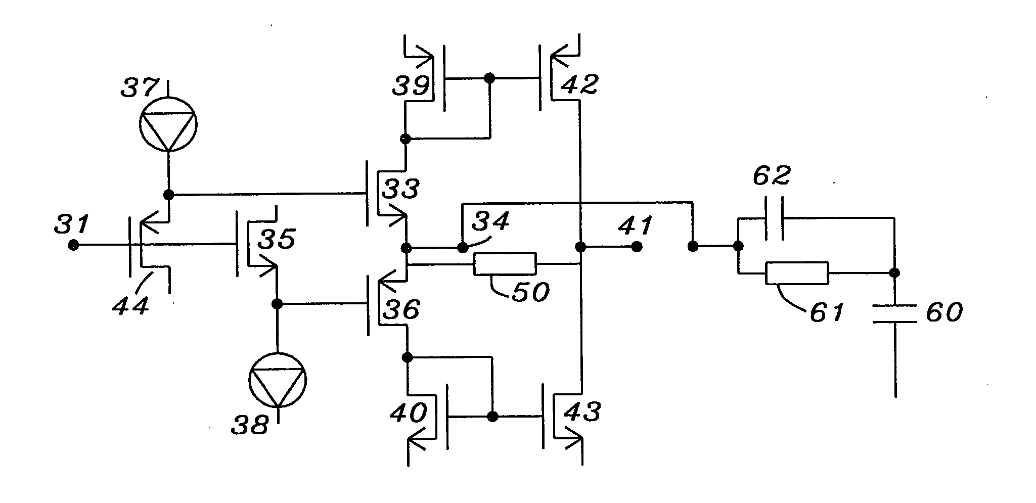
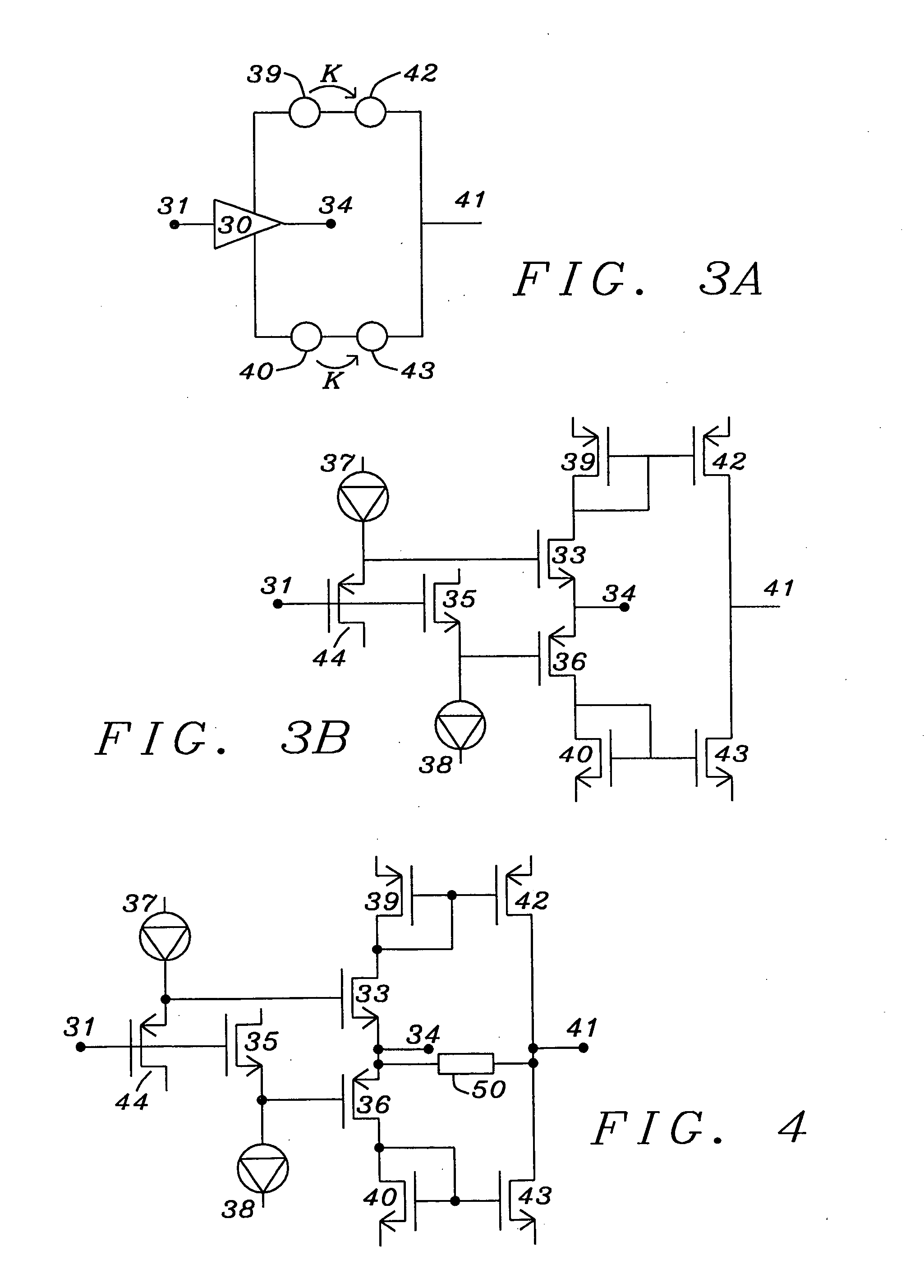
[0032] The preferred embodiments disclose circuits to achieve a buffer amplifier capable to work efficiently in the GHz frequency range. The reverse biased (output to input) isolation of a preferred embodiment is in the area of 20-30 dB. The high isolation is achieved by a 2-stage implementation. For such high frequencies, the output to input isolation is primary dependent on the gate-source capacitance of the active buffer transistor. Having two of said buffer transistors in series and by reducing the impedance between them, a high isolation is achieved.

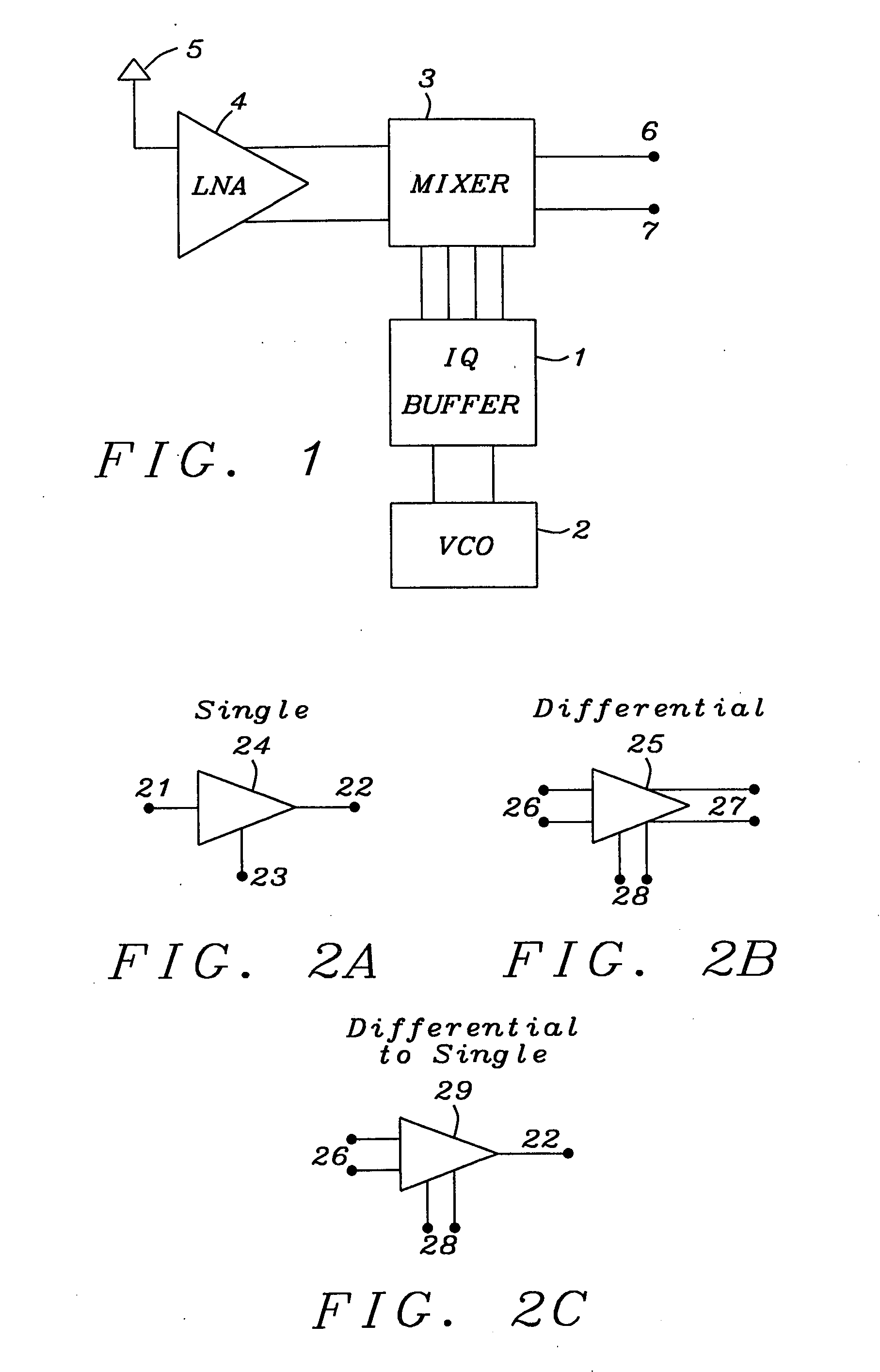
[0033]FIG. 1 shows in a schematic diagram a buffer amplifier 1 hooked up to a voltage-controlled oscillator (VCO) 2 generating signals in the GHz frequency range. Said buffer amplifier is used to amplify e.g. the signals of said VCO and to isolate the VCO from a load connected to the buffer amplifier. Said buffer amplifier is part of a modern wireless communication device comprising also an antenna 5 receiving signals in the GHz fr...


PUM


Abstract

A method and circuits of a high isolation and high-speed buffer amplifier capable to handle frequencies in the GHz range have been achieved. The output to input isolation is primary dependent on the gate-source capacitance of the active buffer transistor. Having two or more in series and by reducing the impedance between them a high isolation can be achieved. The input signals are split in several signal paths and are amplified in the push-pull mode using source follower amplifiers. Then the amplified signals are being combined again. The amplified output current is mirrored applying a multiplication factor. Said method and technology can be used for buffer amplifiers having differential input and differential output or having single input and single output or having differential input and single output. A high reversed biased (output to input) isolation and a reduced quiescent current have been achieved.

Description

BACKGROUND OF THE INVENTION [0001] (1) Field of the Invention [0002] This invention relates generally to high-speed amplifiers and relates more particularly to buffer amplifiers used in communication devices to amplify the signals of a voltage-controlled oscillator (VCO) and to isolate said VCO from a load connected to said amplifier in a frequency range of GHz as for e.g. the Bluetooth technology. [0003] (2) Description of the Prior Art [0004] Modern wireless communication devices use high-frequency signals: 900 MHz to 1900 MHz for cellular phones and higher, up to 6 GHz, for other systems, such as wireless LANs. For example, radios for the “Bluetooth” standard” operate in the unlicensed Industrial, Scientific and Medical (ISM) band at 2.4 GHz. Signals at such frequencies are difficult to generate and to control. They have also a tendency to interfere with each other, as they are easily coupled by parasitic properties present in all electronic components, including integrated circu...

Claims


Application Information

Patent Timeline
Patent Type & Authority Applications(United States)
IPC IPC(8): H03F3/18H03F3/30
CPCH03F3/3028H03F2200/372H03F2200/294H03F3/3059
Inventor SIBRAI, ANDREAS
Owner DIALOG SEMICONDUCTOR GMBH
Why Eureka
Try Eureka