Display apparatus and driving method therefor

a display apparatus and active matrix technology, applied in static indicating devices, instruments, non-linear optics, etc., can solve the problems of reducing transmittance, increasing the density of pixels, and reducing contrast, so as to improve contrast, improve opening ratio, and prevent hysteresis behavior

Inactive Publication Date: 2005-03-10
SONY CORP
View PDF9 Cites 15 Cited by
  • Summary
  • Abstract
  • Description
  • Claims
  • Application Information

AI Technical Summary

Benefits of technology

[0012] Accordingly, in order to solve the problems described above, it is an object of the present invention to provide a configuration of a counter electrode capable of reducing signal amplitude and a driving method for the counter electrode.
[0015] According to the present invention, the counter electrode is not provided as one solid unit but is provided as row counter electrodes divided row by row based on rows of pixels. The row counter electrodes are scanned while a voltage having an opposite phase to a signal input voltage is applied to the row counter electrodes. Thus, a vertical electric field between a counter substrate and a pixel substrate is ensured and a lateral electric field operating between the pixels is moderated. This prevents a defect in orientation of liquid crystal due to local concentration of an electric field between pixels. Furthermore, an increase in the opening ratio, an improvement in the contrast, and prevention of hysteresis behavior in liquid crystal can be achieved. Unlike known VCOM inversion driving, the row counter electrodes divided row by row based on the rows of the pixels are scanned in the present invention. Thus, withstand pressure in a panel can be reduced and the potential of the counter substrate is DC behaved. Therefore, a simple circuit structure can be achieved.
[0016] As described above, providing the row counter electrodes arranged by dividing electrodes on the counter substrate based on the rows of the pixels on the pixel substrate and applying a predetermined potential while scanning the row counter electrodes achieve the effects described below. First, reducing the intensity of an electric field between pixels prevents a defect in orientation of liquid crystal due to disorder of an electric field and reduces a light leakage area. Second, the potential of the signal lines and the potential of the pixels can be reduced, thus enabling a total reduction in the voltage on the pixel substrate. Third, a potential difference between the potential of the signal lines and the potential of the pixels can be reduced, thus enabling a reduction in the leakage of pixel transistors. This significantly prevents an inferior image quality, such as light leakage. Fourth, the amplitude of a signal is reduced and noise inserted from the signal lines via parasitic capacitance is reduced. This significantly prevents an inferior image quality, such as crosstalk, ghost images, and blurring near a border when a window is displayed. Fifth, since a scanning potential of the row counter electrodes arranged on the counter substrate is fixed at positive or negative with respect to a reference potential, a simple circuit structure can be achieved.

Problems solved by technology

As described above, an increase in the density of pixels causes a problem, such as orientation disorder due to a lateral electric field between the pixels.
As a result of this, problems, such as a reduction in the contrast due to orientation disorder, a reduction in the transmittance due to an increase in a light-shielded area to conceal the orientation disorder, hysteresis of liquid crystal molecules due to local concentration of an electric field, and the like occur.
In accordance with an increase in the density, reducing the intensity in an electric field between adjacent pixels is becoming a more important issue.
In addition, large signal amplitude causes various problems.
For example, noise caused by a signal change largely affects pixel potential via parasitic capacitance and this causes inferior image quality, such as crosstalk and blurring or ghost images when a window is displayed.
Also, large signal amplitude causes a large difference between a pixel potential and a signal line potential, and significant leakage of a transistor occurs.
For example, a problem, such as a reduction in the image quality due to light leakage, is caused.
However, actually, inversion driving of a counter electrode formed as one solid unit having a large capacity at a high speed period of 1H is difficult, and this is not practical solving means.

Method used


Image

  • Display apparatus and driving method therefor
  • Display apparatus and driving method therefor
  • Display apparatus and driving method therefor

Examples


Embodiment Construction

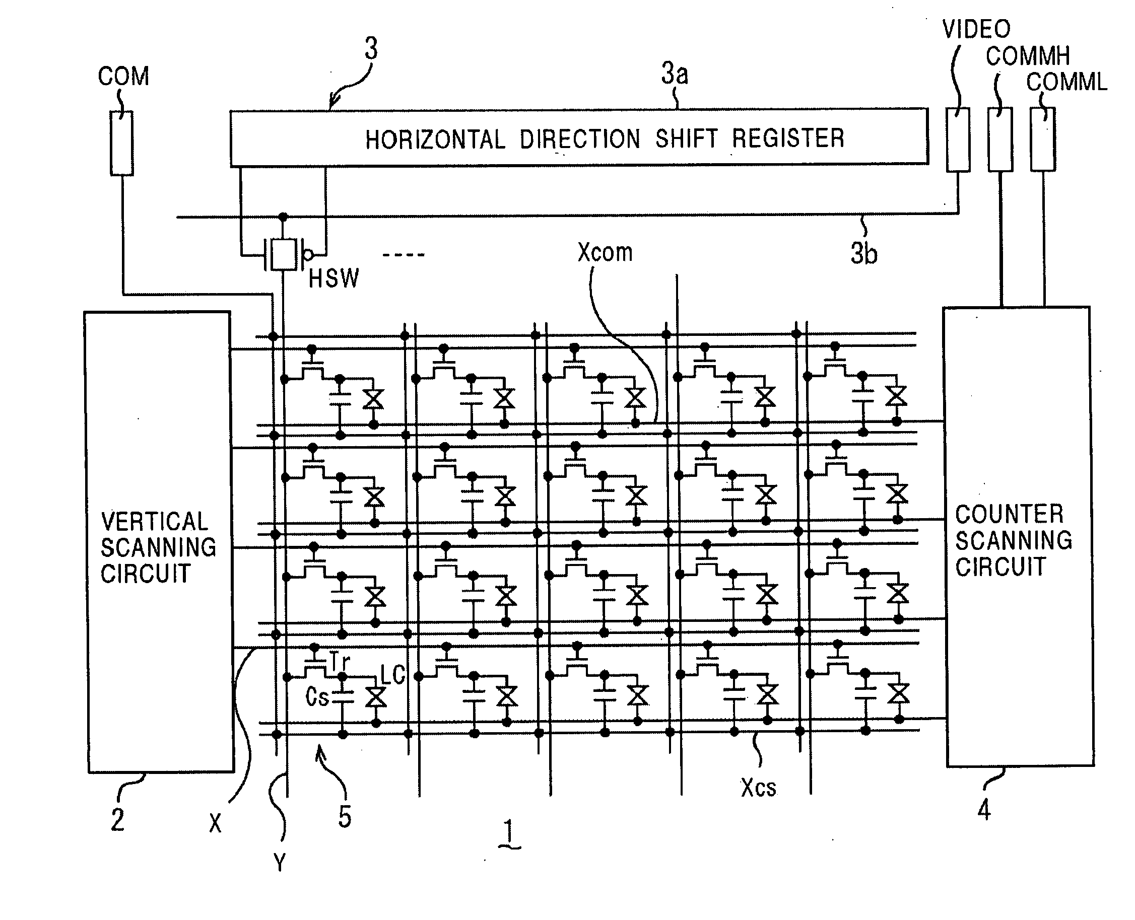
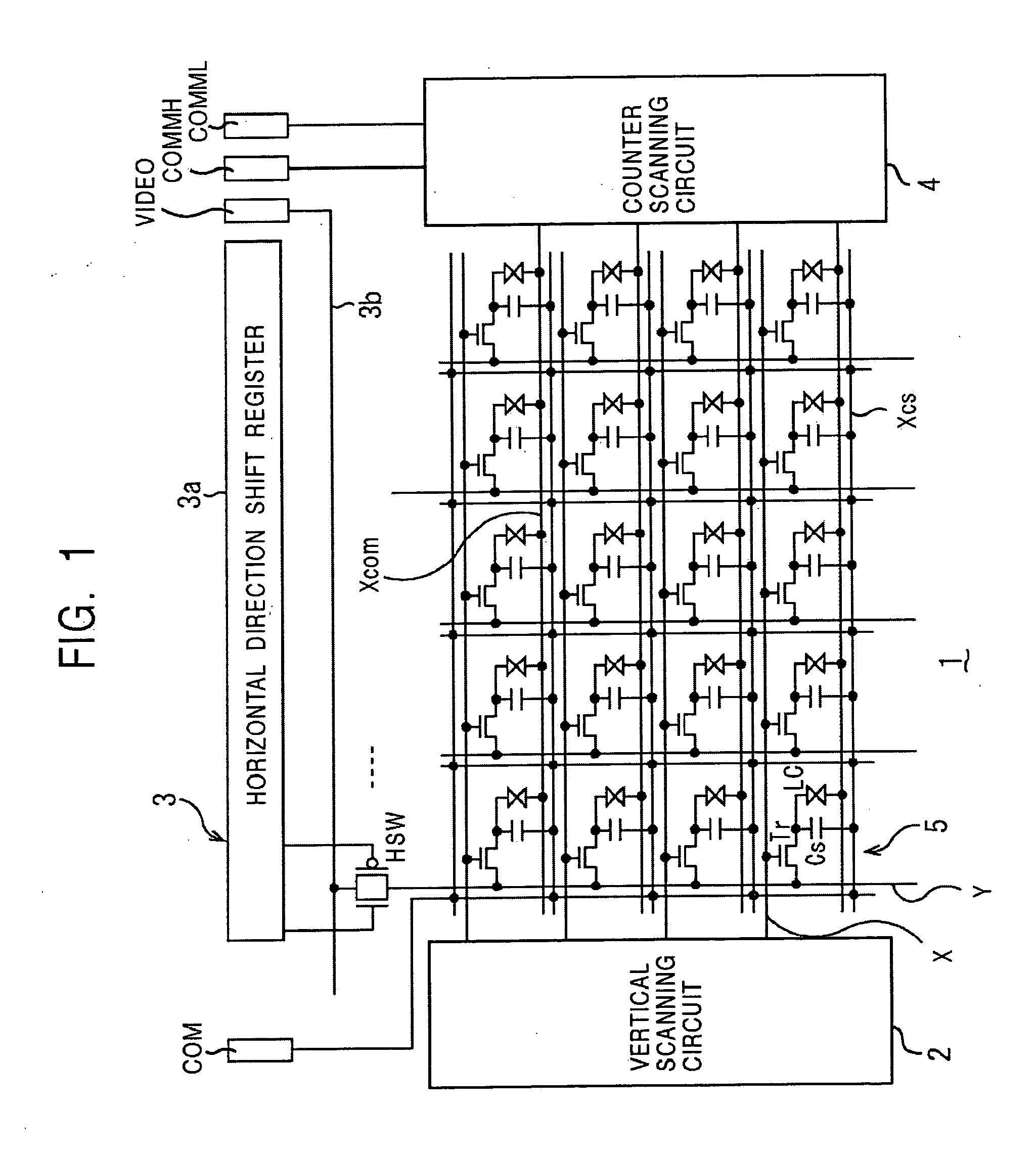
[0024] Embodiments of the present invention will be described with reference to the drawings. FIG. 1 is a circuit block diagram showing the entire structure of a display apparatus according to the present invention. Referring to FIG. 1, the display apparatus basically includes a pixel array unit 1, a vertical scanning circuit 2, and a horizontal driving circuit 3. The pixel array unit 1 includes scanning lines X arranged in rows, signal lines Y arranged in columns, and pixels 5 arranged in a matrix form in association with intersections of the scanning lines X and the signal lines Y. The vertical scanning circuit 2 includes a shift register and the like and is arranged in one side of the pixel array unit 1 to drive the pixel array unit 1. The vertical scanning circuit 2 sequentially applies a selection pulse to each of the scanning lines X so as to sequentially select the pixels 5 row by row. The horizontal driving circuit 3 applies a signal VIDEO whose polarity inverts between high...


PUM

PropertyMeasurementUnit
voltageaaaaaaaaaa
voltageaaaaaaaaaa
voltageaaaaaaaaaa

Abstract

A display apparatus includes pixel electrodes, a counter electrode arranged facing the pixel electrodes, and liquid crystal cells held in a space between the pixel electrodes and the counter electrode. The optical characteristics of the liquid crystal cells change based on potential differences between the pixel electrodes and the counter electrode. The counter electrode includes row counter electrodes divided in accordance with rows of pixels. The display apparatus also includes a counter scanning circuit for sequentially scanning the row counter electrodes in accordance with a pixel row sequentially selected by a vertical scanning circuit and for applying a counter potential of one inverting polarity.

Description

BACKGROUND OF THE INVENTION [0001] 1. Field of the Invention [0002] The present invention relates to active matrix display apparatuses having a flat panel structure, typified by liquid crystal displays (LCDs), and driving methods for the display apparatuses. More particularly, it relates to a configuration of a counter electrode that faces pixel electrodes integratedly formed in a matrix form and a driving method for the counter electrode. [0003] 2. Description of the Related Art [0004]FIG. 6 is a circuit block diagram schematically showing an example of a known display apparatus. Referring to FIG. 6, the display apparatus basically includes a pixel array unit 1, vertical direction shift registers 2a, and a horizontal direction shift register 3a. The pixel array unit 1 includes scanning lines X arranged in rows, signal lines Y arranged in columns, and pixels 5 arranged in a matrix form in association with intersections of the scanning lines X and the signal lines Y. The vertical dir...

Claims


Application Information

Patent Timeline
Patent Type & Authority Applications(United States)
IPC IPC(8): G02F1/1368G02F1/133G09G3/20G09G3/36
CPCG09G3/3655G09G3/3614G02F1/133
Inventor NODA, KAZUHIRO
Owner SONY CORP
Why Eureka
Try Eureka