Wafer-based ion traps

Active Publication Date: 2005-03-24
ARMY GOVERNMENT OF THE UNITED STATES THE AS REPRESENTED BY THE SEC OF THE +1
View PDF9 Cites 31 Cited by
  • Summary
  • Abstract
  • Description
  • Claims
  • Application Information

AI Technical Summary

Benefits of technology

[0011] Various embodiments provide monolithic structures for quadrupole ion traps whose trapping cavities are located in thin layer structures. Each thin layer structure is located on a front surface of a substantially thicker wafer. Thus, the ion traps have linear dimensions that are significantly

Problems solved by technology

Unfortunately, such machining techniques are often complex and cos

Method used


Image

  • Wafer-based ion traps
  • Wafer-based ion traps
  • Wafer-based ion traps

Examples


example 1

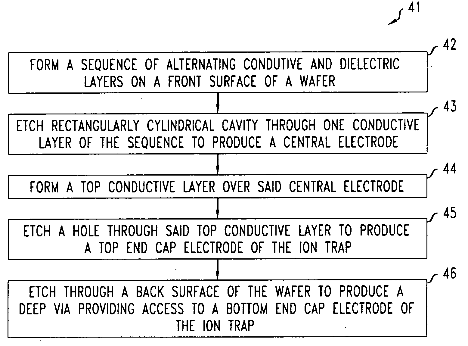
[0043]FIG. 5 illustrates an exemplary method 50 for fabricating a monolithic structure 22′ with an array of micro-ion traps in accordance with method 41 of FIG. 3. The method 50 includes performing first and second sequences of steps I, II from respective front and back surfaces of a silicon (Si) support wafer 23. The steps produce structures 71-77, 22′ of FIGS. 6-13. In FIGS. 6-13, gap “G” indicates portions of the structures 71-77, 22′ that have been omitted for clarity.

[0044] From the front surface of the Si wafer 23, the method 50 includes performing the following sequence of fabrication steps.

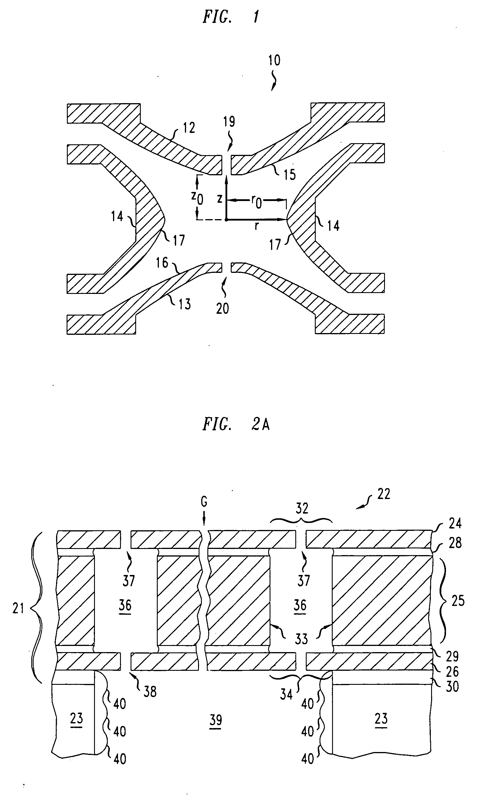
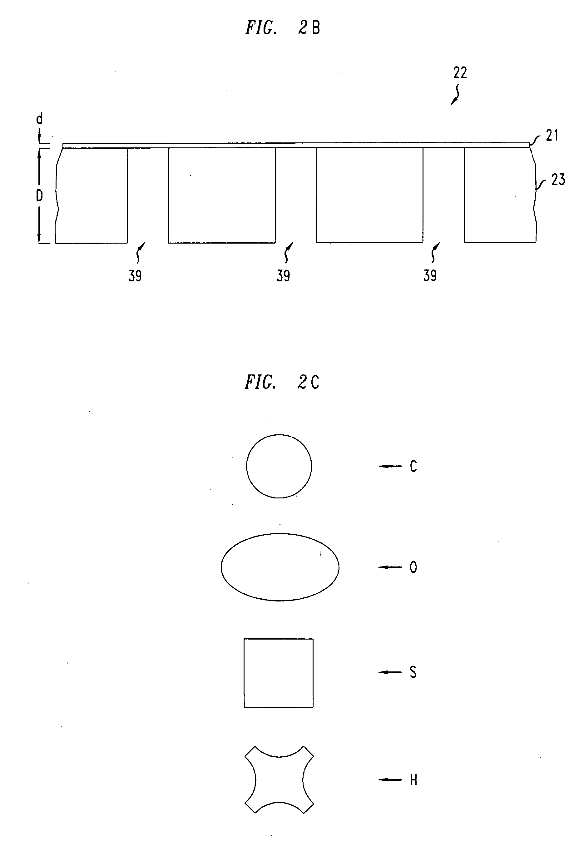
[0045] First, a series of layer depositions on wafer 23 and a series of dry etches produces structure 71 of FIG. 6, which includes a sequence of layers (step 51). The sequence includes a conductive Al layer 90 and relatively thinner dielectric layers 91-92 that surround the Al layer 90. Lateral portions of the Al layer 90 will form bottom end cap electrodes of the final ion traps. The Al...

example 2

[0066] Another exemplary method for fabricating monolithic structure 22′ of FIG. 13 involves modifying method 50 of FIG. 5 by substitutions of different materials. The substitutions involve using doped polysilicon for conductive layers 90, 95, 102 and using either SiO2 or a spin on curable polymer for the sacrificial material of step 54. For such substitutions, the sequence of front side steps entails the following changes. The depositions for the conductive material of layers 90, 95, 102 involve performing plasma enhanced CVD depositions for polysilicon doped n-type or p-type with concentrations of 1019 or more dopant atoms per cm3. The dry etches that form features in the conductive material of the doped polysilicon layers 90, 95,102 involve performing conventional RIE plasma etches that are adapted to selectively remove polysilicon. The CMP for planarizing the top surface 101 of intermediate structure 74 of FIG. 9 uses a chemical polishing agent that selectively removes the SiO2 ...


PUM

PropertyMeasurementUnit
Heightaaaaaaaaaa
Thicknessaaaaaaaaaa
Electrical conductoraaaaaaaaaa

Abstract

An apparatus for an ion trap includes a semiconductor or dielectric wafer with front and back surfaces, a sequence of alternating conductive and dielectric layers formed over said front surface, and a bottom conductive layer. The sequence includes top and middle conductive layers, wherein the middle conductive layer is closer to the wafer than the top conductive layer. The middle conductive layer includes a substantially right cylindrical cavity that crosses a width of the middle conductive layer. The top and bottom conductive layers cap respective first and second ends of the cavity. The top conductive layer includes a hole that forms a first access port to the cavity. The wafer includes via through the width of the wafer. The via provides another access to the cavity via the back surface of the wafer. The wafer is substantially thicker than the sequence of layers.

Description

BACKGROUND [0001] 1. Field of the Invention [0002] This invention relates to ion traps and to methods for fabricating ion traps. [0003] 2. Description of the Related Art [0004] Conventional ion traps enable both storing ionized particles and separating the stored ionized particles according to their mass (M) to charge (Q) ratios. Storing the ionized particles involves applying a time-varying voltage to the ion trap so that particles propagate along stable trajectories therein. Separating the ionized particles typically involves applying an additional time-varying voltage to the trap so that the stored particles are selectively ejected according to their M / Q ratios. The ability to eject particles according to their M / Q ratios enables the use of ion traps as mass spectrometers. [0005] Exemplary ion traps are described, e.g., in U.S. Pat. No. 2,939,952, issued Jun. 7, 1960 to W. Paul et al, which is incorporated herein by reference in its entirety. [0006]FIG. 1 shows one type of quadru...

Claims


Application Information

Patent Timeline
IPC IPC(8): B81B1/00H01J49/42C23F1/00H01J49/26
CPCB81B1/00H01J49/424H01J49/0018
Inventor PAI, CHIEN-SHINGPAU, STANLEY
Owner ARMY GOVERNMENT OF THE UNITED STATES THE AS REPRESENTED BY THE SEC OF THE
Why Eureka
Try Eureka