Photovoltaic cell and method of fabricating the same

Active Publication Date: 2005-03-24
SANYO ELECTRIC CO LTD
View PDF5 Cites 158 Cited by
  • Summary
  • Abstract
  • Description
  • Claims
  • Application Information

AI Technical Summary

Benefits of technology

[0010] It is an object of the present invention to provide a photovoltaic cell and

Problems solved by technology

At the junction of the n-type single-crystalline substrate and the p-type amorphous silicon film, however, there are multiple interface states, causing recombination of carriers to lower the open-circuit voltage Voc.
In the above photovoltaic cell, however, the electrode and the p-type amorphous silicon film on the main-surface sid

Method used


Image

  • Photovoltaic cell and method of fabricating the same
  • Photovoltaic cell and method of fabricating the same
  • Photovoltaic cell and method of fabricating the same

Examples


first embodiment

[0078] A first embodiment of the present invention will hereinafter be described.

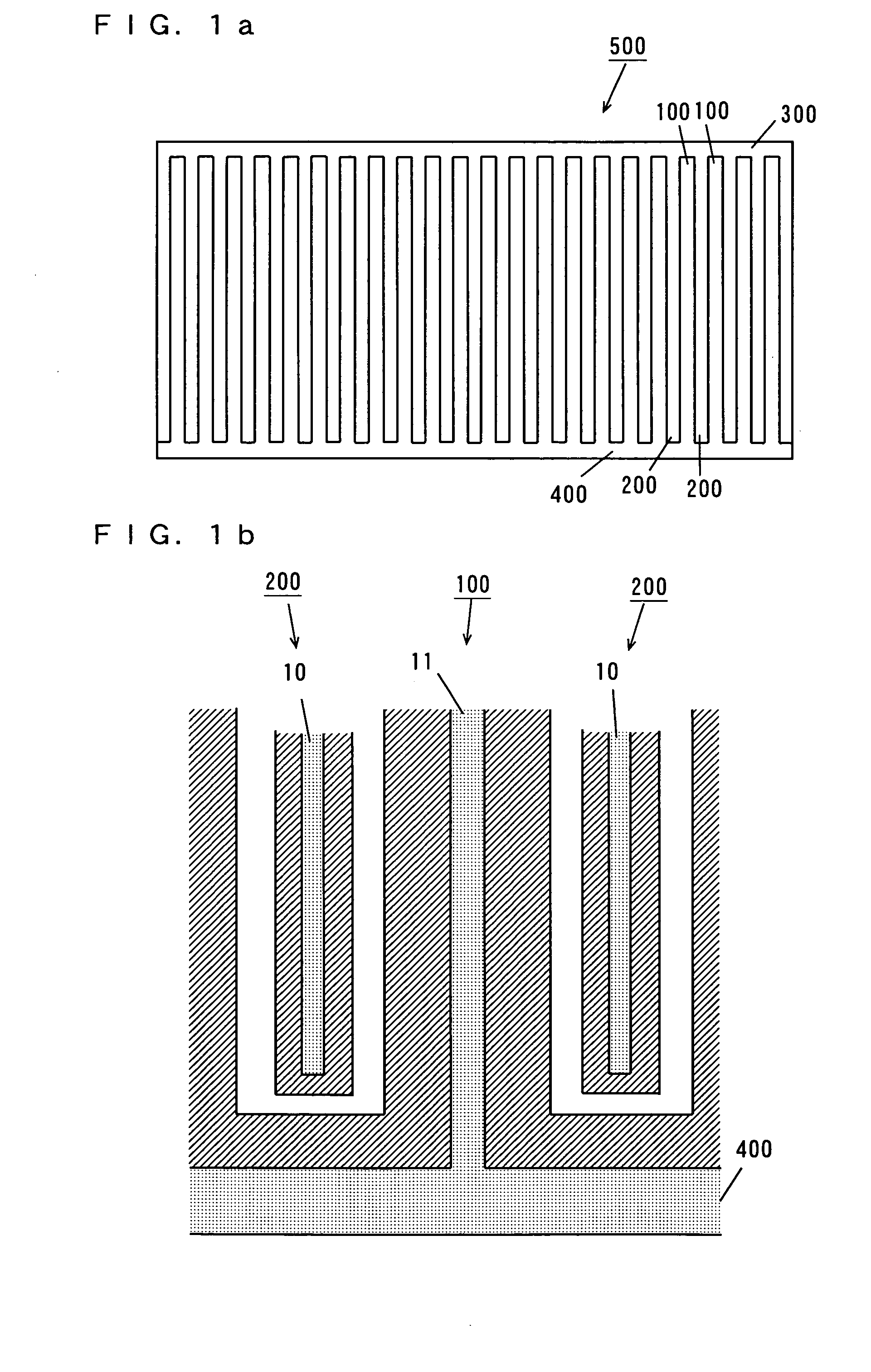
[0079]FIG. 1a is a plan view showing the back surface of a photovoltaic cell 500 according to this embodiment, and FIG. 1b is a partly enlarged view of FIG. 1a.

[0080] As shown in FIG. 1a, the photovoltaic cell 500 has a rectangular shape with its shorter side being 5 cm and longer side 10 cm, for example. The back surface of the photovoltaic cell 500 comprises positive electrodes 100 and negative electrodes 200 in a comb-shape. The positive electrodes 100 and negative electrodes 200 align alternately, each extending in the direction of the shorter side of the photovoltaic cell 500. Electrodes 300, 400 are also provided along the respective longer sides of the back surface of the photovoltaic cell 500.

[0081] As shown in FIG. 1b, the positive electrode 100 and the negative electrode 200 are provided with collector electrodes 11, 10, respectively. The collector electrode 10 is connected to the positive ...

second embodiment

[0101] A second embodiment of the present invention will hereinafter be described.

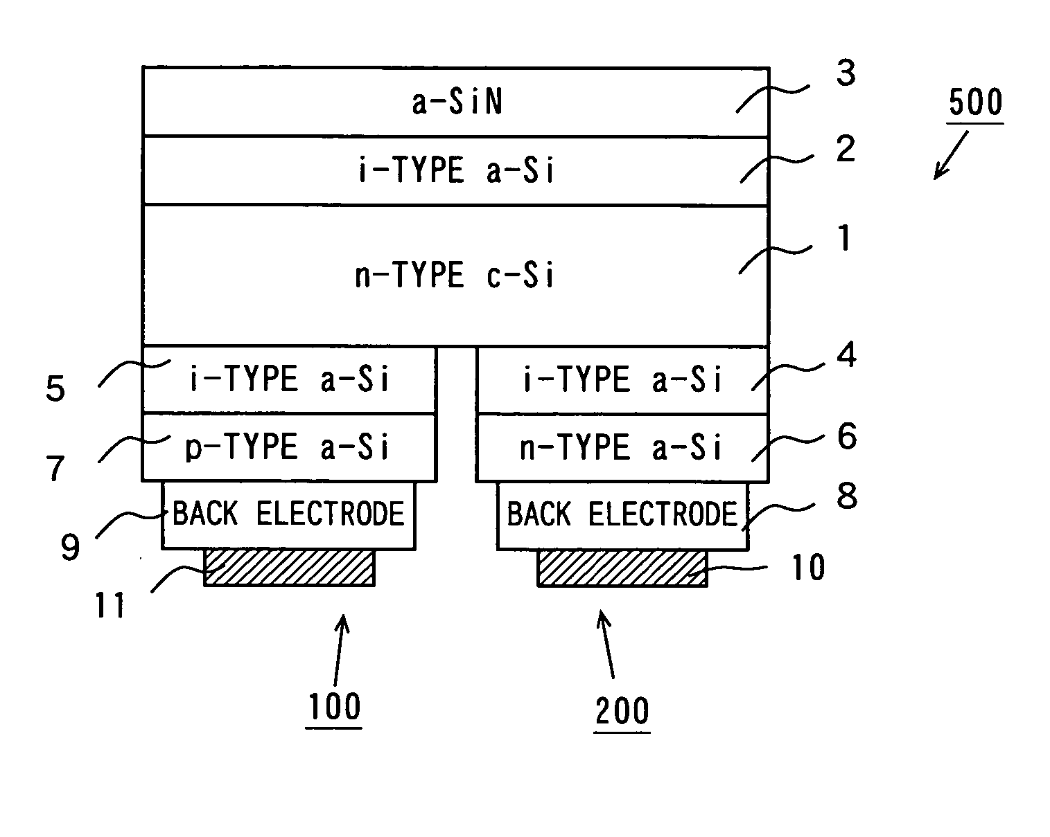
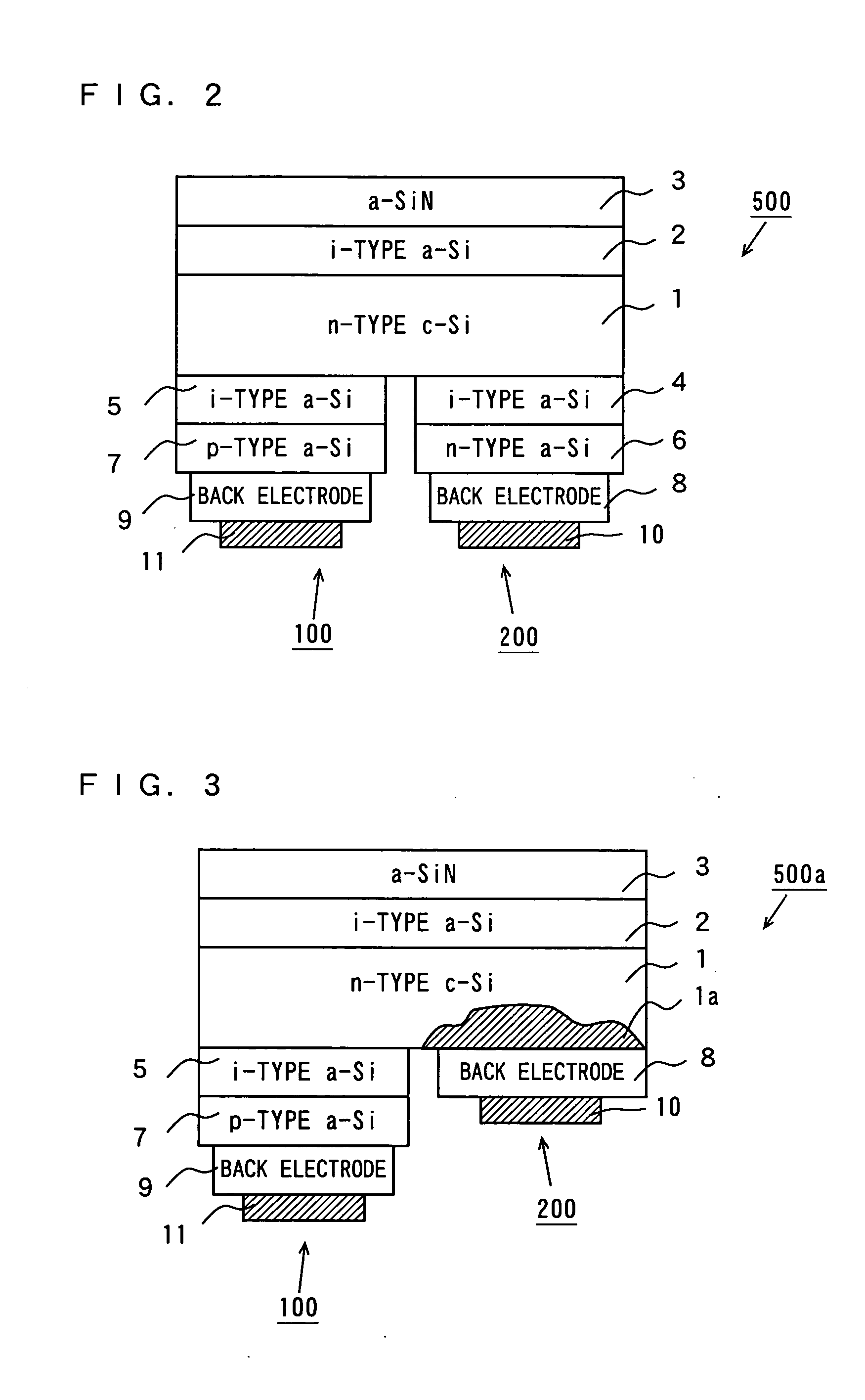
[0102]FIG. 3 is a schematic cross section showing the structure of a photovoltaic cell 500a according to the second embodiment. The photovoltaic cell 500a of FIG. 3 differs from the photovoltaic cell 500 of FIG. 1 in that it comprises impurities diffusion layer 1a in an n-type single-crystalline silicon substrate 1, instead of the i-type amorphous silicon film 4 and the n-type amorphous silicon film 6.

[0103] The impurity diffusion layer 1a is formed by thermal diffusion of P (phosphor) with high concentration on part of the region of the back surface of the n-type single-crystalline silicon substrate 1 where an i-type amorphous silicon film 5 is not formed. Then, a back electrode 8 and a collector electrode 10 are formed on the impurity diffusion layer 1a.

[0104] In this embodiment, it is not necessary to form an i-type amorphous silicon film 4 and an n-type amorphous silicon film 6 in the fabricatio...

third embodiment

[0105] A third embodiment of the present invention will hereinafter be described.

[0106]FIG. 4 is a schematic cross section showing the structure of a photovoltaic cell 500b according to the third embodiment. The photovoltaic cell 500b of FIG. 4 differs from the photovoltaic cell 500 of FIG. 1 in that an i-type amorphous silicon film 4 is in contact with an end of a p-type amorphous silicon film 7.

[0107] The method of fabricating the photovoltaic cell 500b will now be described. The method of forming an i-type amorphous silicon film 2 and an anti-reflection film 3 on the main-surface side of an n-type single-crystalline silicon substrate 1, and an i-type amorphous silicon film 5 and a p-type amorphous silicon film 7 on the back-surface side thereof is the same as that for the photovoltaic cell 500 of FIG. 2.

[0108] At the time of formation of the i-type amorphous silicon film 4 and n-type amorphous silicon film 6, a metal mask is coated so that its end face is aligned with the end ...


PUM


Abstract

An i-type amorphous silicon film and an anti-reflection film made of amorphous silicon nitride or the like are formed in this order on a main surface of an n-type single-crystalline silicon substrate. On a back surface of the n-type single-crystalline silicon substrate are provided a positive electrode and a negative electrode next to each other. The positive electrode includes an i-type amorphous silicon film, a p-type amorphous silicon film, a back electrode, and a collector electrode formed in this order on the back surface of the n-type single-crystalline silicon substrate. The negative electrode includes an i-type amorphous silicon film, an n-type amorphous silicon film, a back electrode, and a collector electrode formed in this order on the back surface of the n-type single-crystalline silicon substrate.

Description

BACKGROUND OF THE INVENTION [0001] 1. Field of the Invention [0002] The present invention relates to a photovoltaic cell using a semiconductor junction and a method of fabricating the same. [0003] 2. Description of the Background Art [0004] In recent years, a photovoltaic cell having a junction of an n-type single-crystalline silicon substrate and a p-type amorphous silicon film has been developed. In order to enhance photoelectric conversion efficiency of such a photovoltaic cell, it is necessary to enhance fill factor F.F. while maintaining high short-circuit current Isc and open-circuit voltage Voc. [0005] At the junction of the n-type single-crystalline substrate and the p-type amorphous silicon film, however, there are multiple interface states, causing recombination of carriers to lower the open-circuit voltage Voc. [0006] For this reason, in order to suppress such recombination of carriers at the junction of an n-type single-crystalline silicon substrate and a p-type amorphou...

Claims


Application Information

Patent Timeline
IPC IPC(8): H01L31/075
CPCH01L31/0747Y02E10/548H01L31/075H01L31/022441Y02E10/50
Inventor TERAKAWA, AKIRAASAUMI, TOSHIO
Owner SANYO ELECTRIC CO LTD
Why Eureka
Try Eureka