Vertically-stacked co-planar transmission line structure for IC design

a transmission line and coplanar technology, applied in the direction of waveguides, semiconductor devices, semiconductor/solid-state device details, etc., can solve the problems of inferior loss and reflection characteristics, and achieve the effect of superior performan

Inactive Publication Date: 2005-03-24
IBM CORP
View PDF7 Cites 13 Cited by
  • Summary
  • Abstract
  • Description
  • Claims
  • Application Information

AI Technical Summary

Benefits of technology

[0010] The on-chip stacked coplanar micro-strip/waveguides of the present invention allow chip designers to design a much wider range of characteristic impedances, and also provide dramatic improvements in insertion loss and reflection loss to low-impedance sou

Problems solved by technology

Conventional on-chip transmission lines are routed in a single metal layer in an IC chi

Method used


Image

  • Vertically-stacked co-planar transmission line structure for IC design
  • Vertically-stacked co-planar transmission line structure for IC design
  • Vertically-stacked co-planar transmission line structure for IC design

Examples


Embodiment Construction

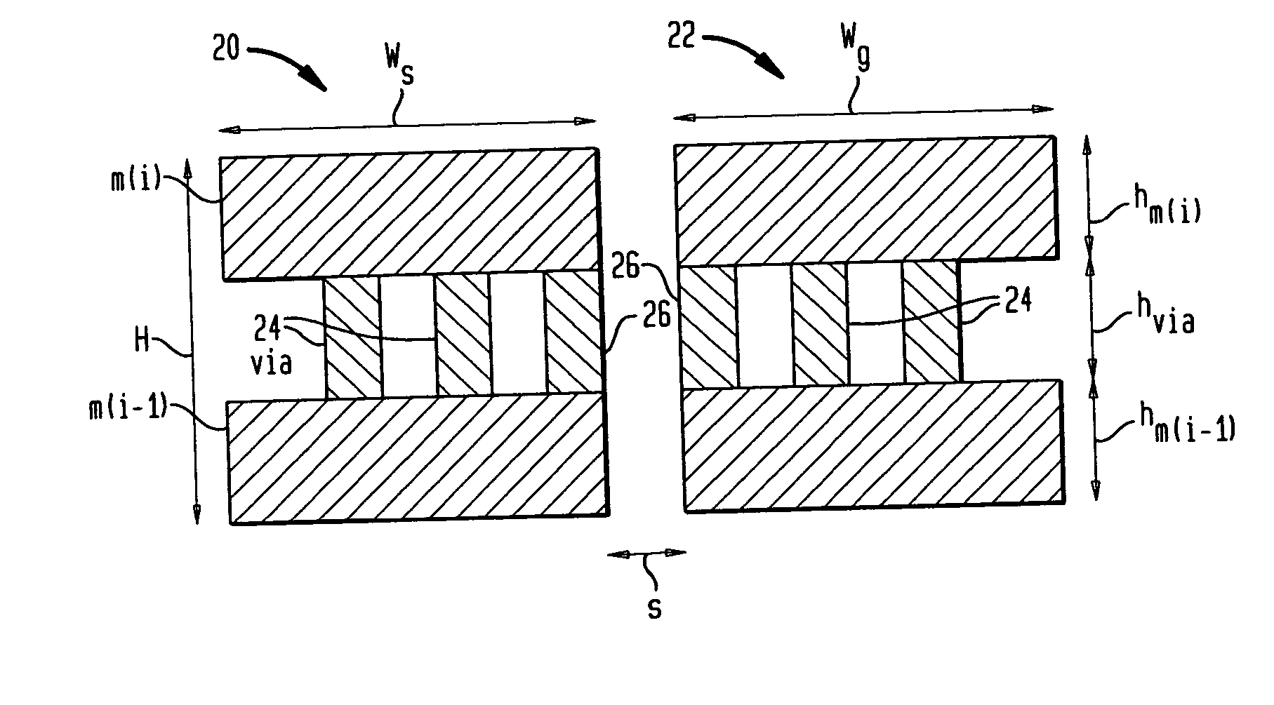
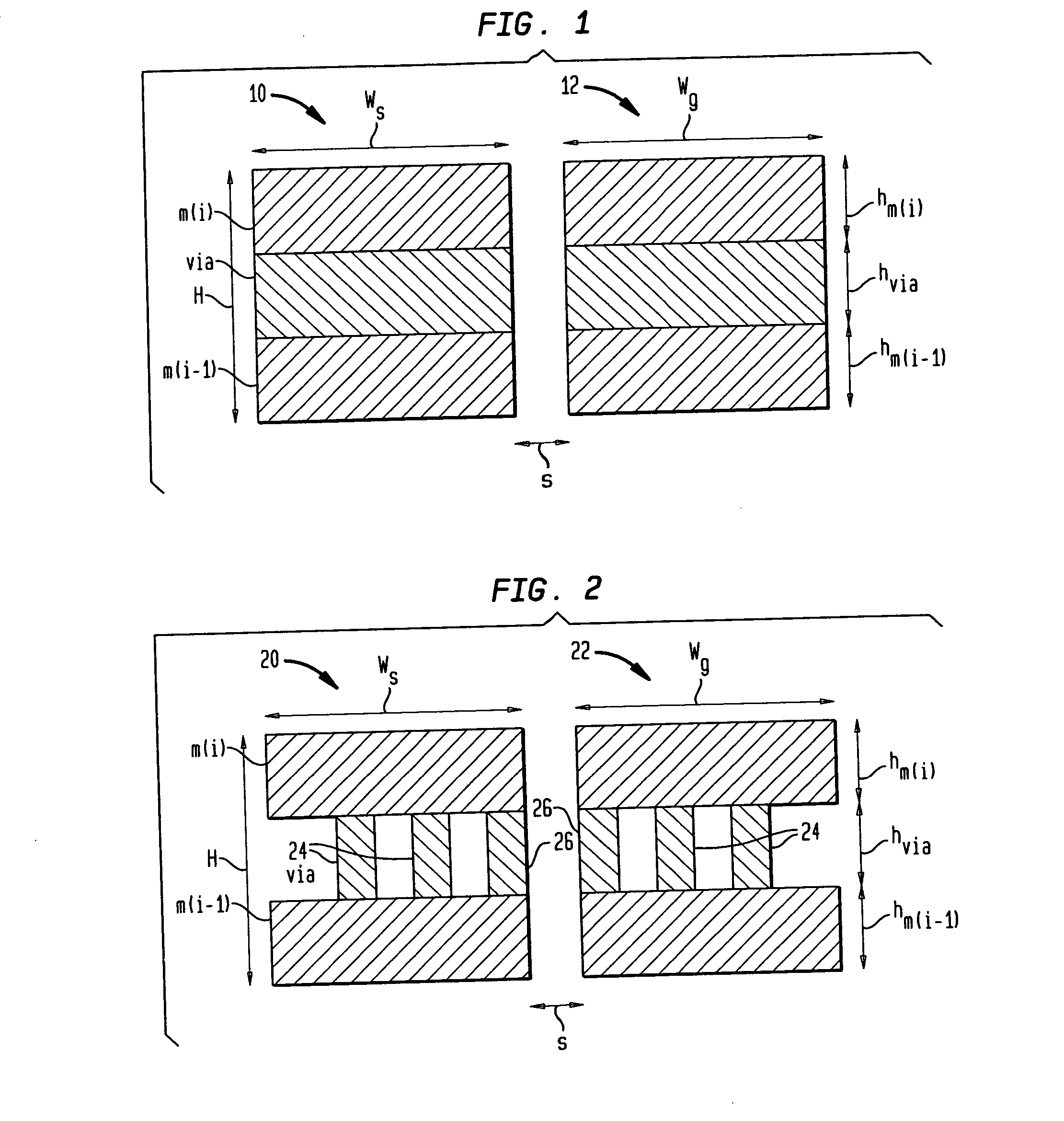
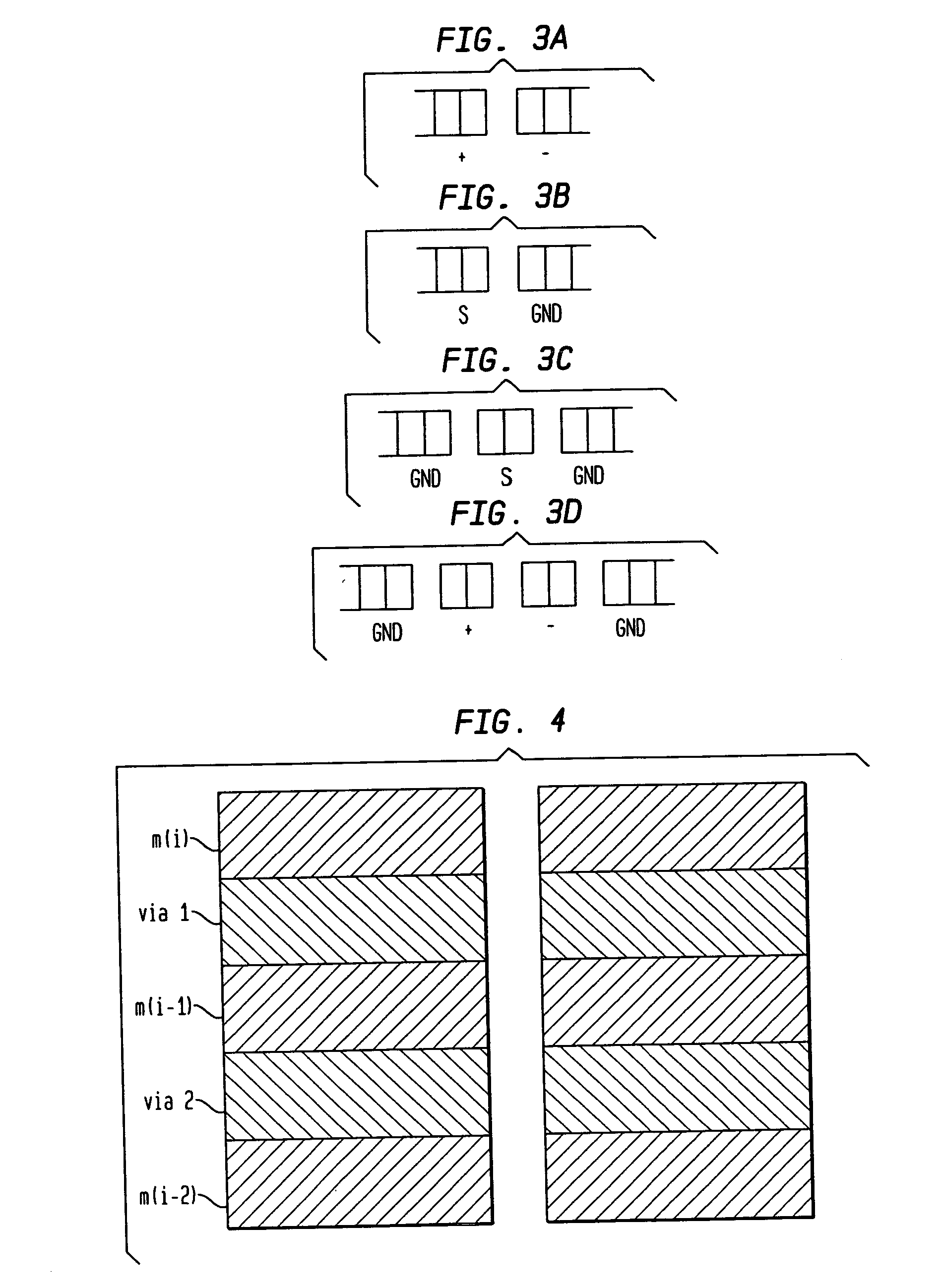
[0018] The present invention provides new on-chip transmission line designs that have superior loss and reflection characteristics relative to conventional on-chip transmission line approaches. In the context of the present invention, a transmission line is defined as a waveguide interconnect structure having two or more conductors and defining a closed ground return path within the waveguide interconnect structure.

[0019] Conventional on-chip transmission lines are routed in a single metal layer in the chip's metal-dielectric stack. In contrast thereto, the transmission line design of the present invention consists of metal lines in multiple metal and via levels in the chip's metal-dielectric stack. The simplest structure is a metal transmission line that is comprised of a metal layer, the next metal layer down, and the via metal in between the two metal layers (all with equal width and length dimensions). This structure can either be a coplanar differential pair of conductors as s...


PUM


Abstract

A vertically stacked coplanar transmission line structure for an IC (integrated circuit) is provided which has superior loss and reflection characteristics relative to conventional on-chip transmission line designs. A simple embodiment of the vertically stacked coplanar transmission line structure comprises a micro-strip pair of first and second vertically stacked coplanar conductors, each comprising a metal layer, a next metal layer down, and an intermediate connecting via layer in between the metal layer and the next metal layer down.

Description

BACKGROUND OF THE INVENTION [0001] 1. Field of the Invention [0002] The present invention relates generally to a vertically-stacked co-planar transmission line structure for an IC (integrated circuit) design, and more particularly pertains to on-chip transmission line designs that have superior loss and reflection characteristics relative to conventional on-chip transmission line designs. [0003] 2. Discussion of the Prior Art [0004] Conventional on-chip transmission lines are routed in a single metal layer in an IC chip's metal-dielectric stack which result in inferior loss and reflection characteristics. [0005] Stacked conductors have been used in prior art on-chip spiral stacked inductor designs. In these designs, the lower resistance of the stacked conductors results in higher Qs (quality factors) for the spiral inductors. [0006] During operation of prior art on-chip spiral stacked inductors, most of the current flowing in the conductors is located against the inside edges (edges...

Claims


Application Information

Patent Timeline
IPC IPC(8): H01L21/82H01L21/822H01L27/04H01L23/522H01L23/66H01P3/02
CPCH01L23/5222H01L23/66H01L2924/3011H01L2924/0002H01L2924/00
Inventor SINGH, RAMINDERPALTRETIAKOV, YOURI V.VAED, KUNALWOODS, WAYNE H. JR.
Owner IBM CORP
Why Eureka
Try Eureka