Method of forming closed air gap interconnects and structures formed thereby

a metal-insulator and air gap technology, applied in the direction of electrical equipment, semiconductor devices, semiconductor/solid-state device details, etc., can solve the problems of affecting the speed and thereby chip performance of the chip, the difficulty of placing a bridge layer on top of the extracted structure, and the general difficulty of reducing to practice, so as to maximize the air gap volume fraction, increase the performance, and minimize the amount of unsupported wiring

Inactive Publication Date: 2005-03-24
TAIWAN SEMICON MFG CO LTD
View PDF28 Cites 188 Cited by
  • Summary
  • Abstract
  • Description
  • Claims
  • Application Information

AI Technical Summary

Benefits of technology

[0024] Another object of the present invention is to provide an air gap-containing interconnect structure which maximizes air gap volume fraction (relative to total volume fraction of dielectric), while minimizing the amount of unsupported wiring thus increasing the performance.
[0025] Another object of the present invent

Problems solved by technology

Through their effects on signal propagation delays, the materials and layout of these interconnect structures can substantially impact chip speed and thereby chip performance.
This is generally very difficult to reduce to practice.
If extraction is performed without a bridge layer being present in the structure as a means of bypassing this difficulty of extracting layers through a semi-permeable medium, it would be very difficult to place a bridge layer on top of the extracted structure.
A further concern with air gap dielectrics is that they leave metal wiring features more susceptible to the opens and shorts induced by electromigration-driven mass tran

Method used


Image

  • Method of forming closed air gap interconnects and structures formed thereby
  • Method of forming closed air gap interconnects and structures formed thereby
  • Method of forming closed air gap interconnects and structures formed thereby

Examples


first embodiment

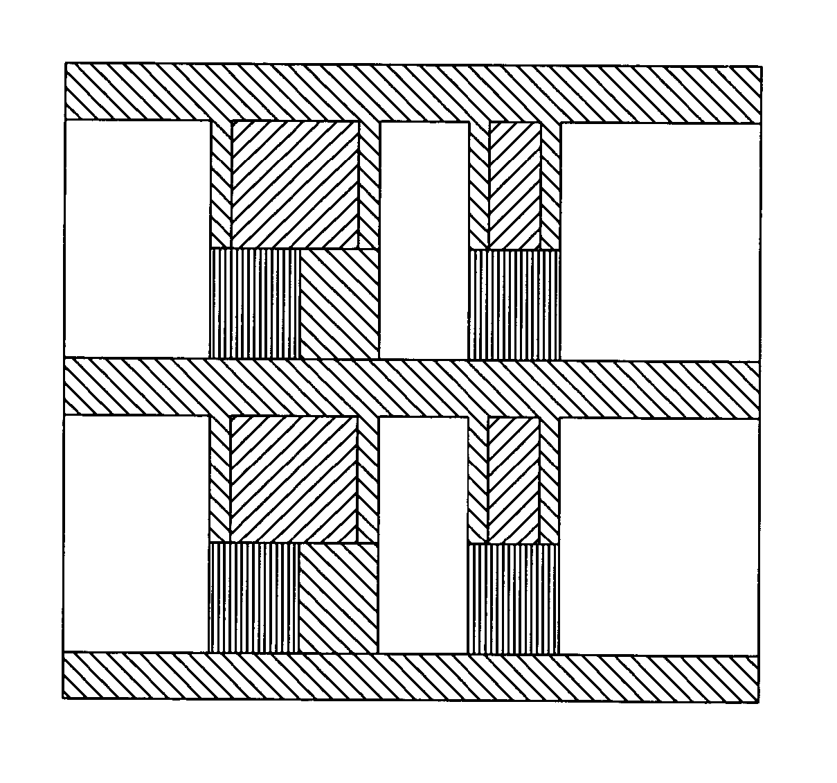
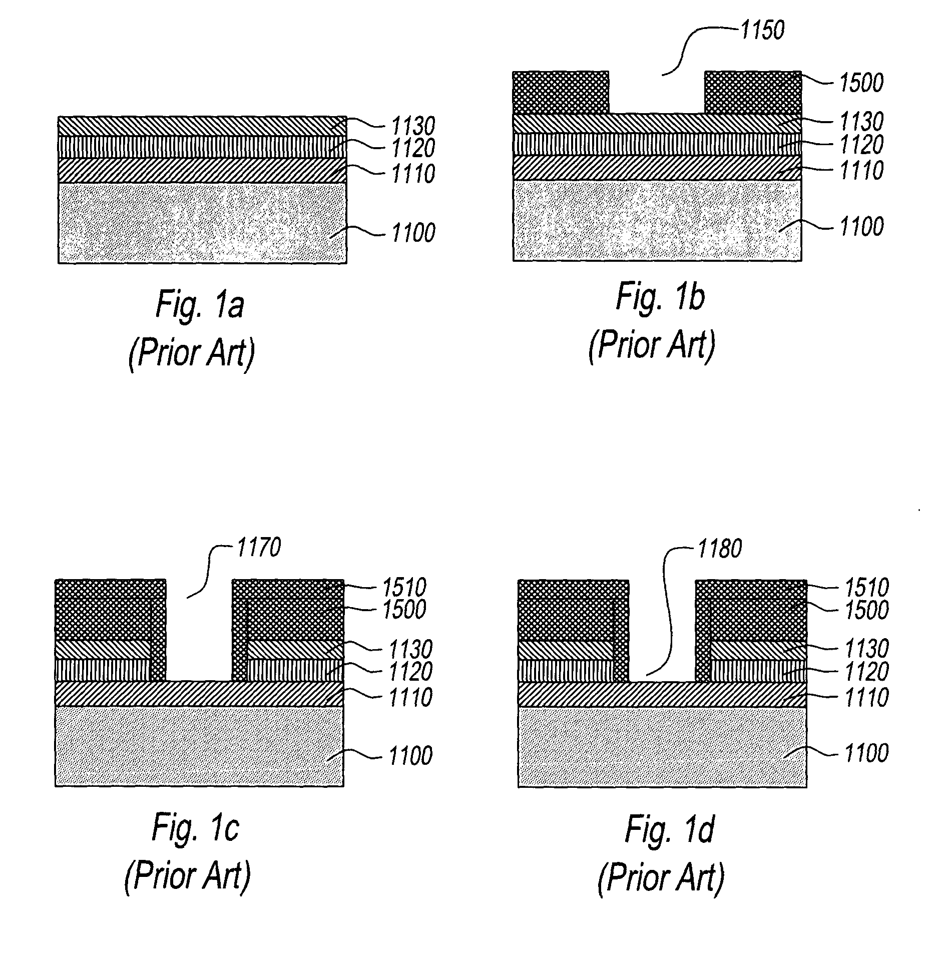
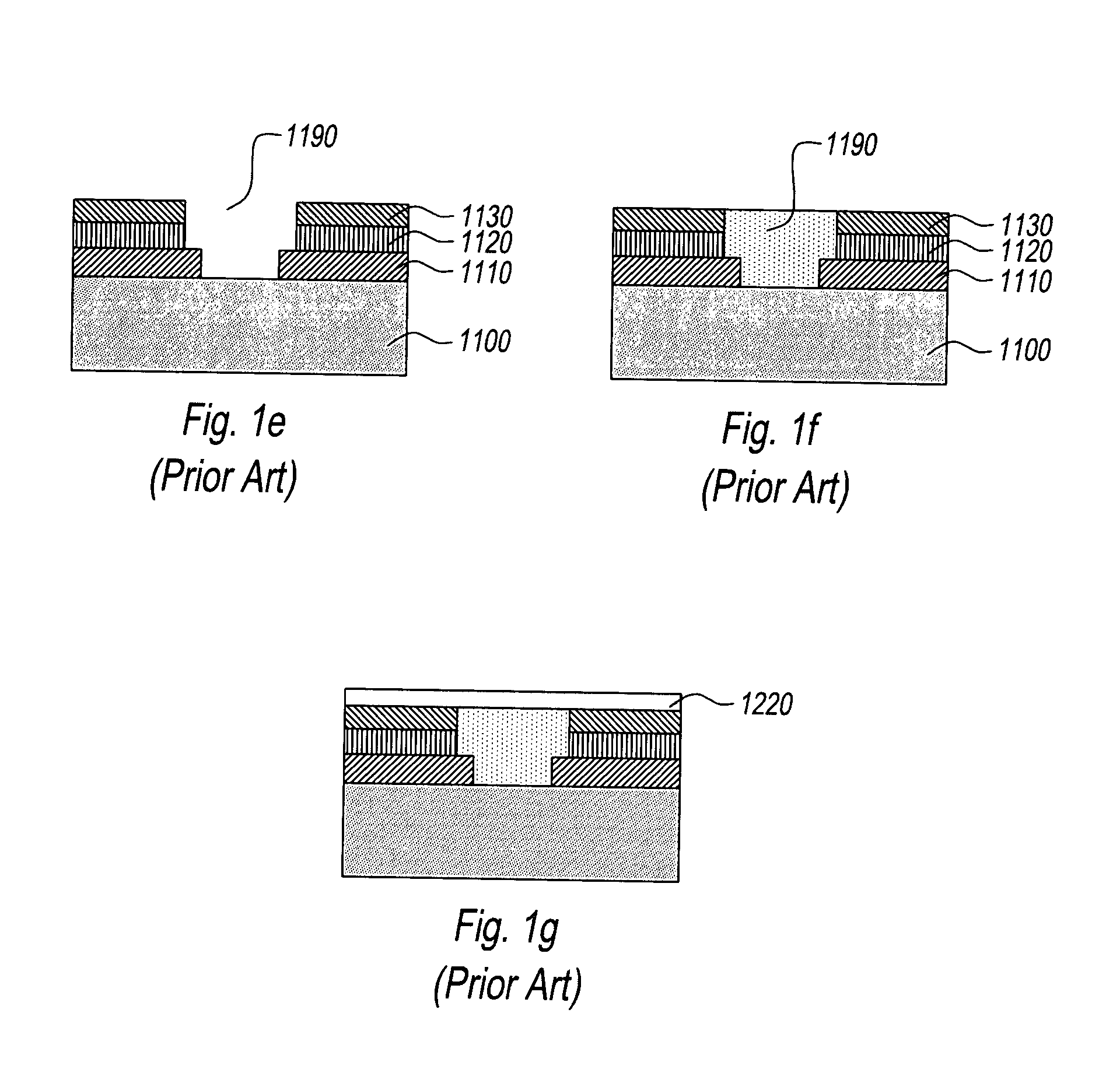
[0045] In the interconnect structure, the stencil with holes stays in place, holes are closed off by a cap dielectric. The structure has no hard mask or conformal dielectric passivation. The closed air gap interconnect structure includes: a substrate; a first sacrificial dielectric coated on the substrate, the first coated sacrificial dielectric having therein a patterned set of support regions formed by lithography and filled and planarized with a robust line support dielectric, the first sacrificial dielectric having therein contact via holes patterned by reactive ion etching; a second sacrificial dielectric coated on the first sacrificial dielectric and the filled and planarized support regions, the second sacrificial dielectric having lithographically patterned line trenches; a conductive material filled into the line trenches and the via holes and planarized; and a stencil with a regular array of holes on the filled line trenches and the second sacrificial dielectric wherein th...

fourth embodiment

[0048] In the interconnect structure, the stencil with holes stays in place and the structure has a selective metal cap. The holes are closed off by a cap dielectric. The structure has no hard mask or conformal dielectric passivation. The closed air gap interconnect structure includes a substrate; a first sacrificial dielectric coated on the substrate, the first coated sacrificial dielectric having therein a patterned set of support regions by lithography and filled and planarized with a robust line support dielectric, the first sacrificial dielectric having therein contact via holes patterned by reactive ion etching; a second sacrificial dielectric coated on the first sacrificial dielectric and the filled and planarized support regions, the second sacrificial dielectric having lithographically patterned line trenches; a conductive material filled into the line trenches and the via holes and planarized; an optional conductive material cap disposed on top surfaces of the conductive m...


PUM


Abstract

A method to form a closed air gap interconnect structure is described. A starting structure made of regions of a permanent support dielectric under the interconnect lines and surrounding interconnect vias with one or more sacrificial dielectrics present in the remaining portions of the interconnect structure, is capped with a dielectric barrier which is perforated using a stencil with a regular array of holes. The sacrificial dielectrics are then extracted through the holes in the dielectric barrier layer such that the interconnect lines are substantially surrounded by air except for the regions of the support dielectric under the lines. The holes in the cap layer are closed off by depositing a second barrier dielectric so that a closed air gap is formed. Several embodiments of this method and the resulting structures are described.

Description

BACKGROUND OF THE INVENTION [0001] 1. Field of the Invention [0002] The present invention relates to ultra low dielectric constant (ULK) and air gap-containing metal-insulator interconnect structures for Very Large Scale Integrated (VLSI) and Ultra-Large Scale Integrated (ULSI) devices and packaging. More particularly, the present invention relates to structures, methods, and materials relating to the incorporation of ULK materials and air gaps into multiple levels of multilayer interconnect structures. [0003] 2. Description of the Prior Art [0004] Device interconnections in Very Large Scale Integrated (VLSI) or Ultra-Large Scale Integrated (ULSI) semiconductor chips typically have multilevel structures containing patterns of metal wiring layers that are encapsulated in an insulator. Wiring structures within a given level of wiring are separated by an intralevel dielectric, whereas the individual wiring levels are separated from each other by layers of an interlevel dielectric. Cond...

Claims


Application Information

Patent Timeline
IPC IPC(8): H01L21/768H01L23/522H01L23/532
CPCH01L21/76807H01L21/7682H01L23/5222H01L23/53238H01L2924/0002H01L23/5329H01L2924/00
Inventor SAENGER, KATHERINE L.SURENDRA, MAHESWARANKARECKI, SIMON M.NITTA, SATYA V.PURUSHOTHAMAN, SAMPATHCOLBURN, MATTHEW E.DALTON, TIMOTHY J.HUANG, ELBERT
Owner TAIWAN SEMICON MFG CO LTD
Why Eureka
Try Eureka