Plasma display panel and method for manufacturing the same

a technology of display panel and plasma, which is applied in the manufacture of electric discharge tubes/lamps, electrodes, and electrode systems, etc., can solve the problems of shortened lifespan of protection films, fine cracks on the surface of protection films, and damage to dielectric films

Inactive Publication Date: 2005-03-24
LG ELECTRONICS INC
View PDF2 Cites 1 Cited by
  • Summary
  • Abstract
  • Description
  • Claims
  • Application Information

AI Technical Summary

Benefits of technology

[0011] Accordingly, the present invention has been made in view of the above problems, and it is an object of the present invention

Problems solved by technology

Due to this, the dielectric film is damaged.
Accordingly, fine cracks are created on the surface of the protection film due to shock of the plasma particles.
Thus, there are problems in that the lifespan of the protection film is shortened and a probability of emitting secondary electrons ge

Method used


Image

  • Plasma display panel and method for manufacturing the same
  • Plasma display panel and method for manufacturing the same
  • Plasma display panel and method for manufacturing the same

Examples


first embodiment

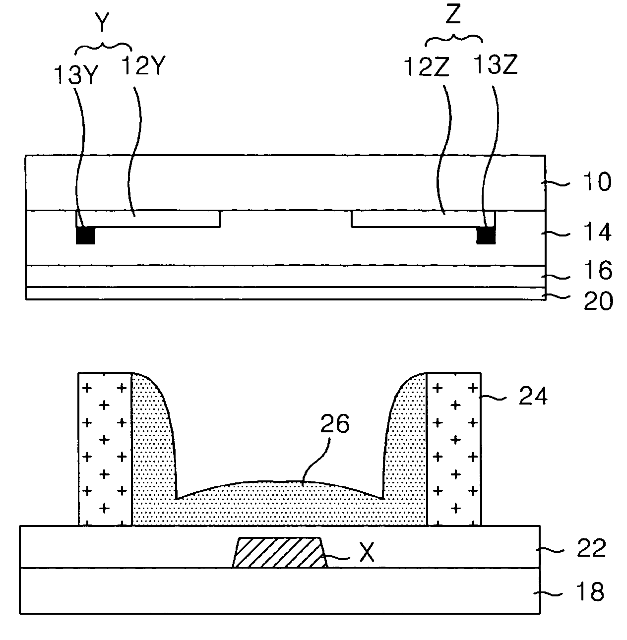
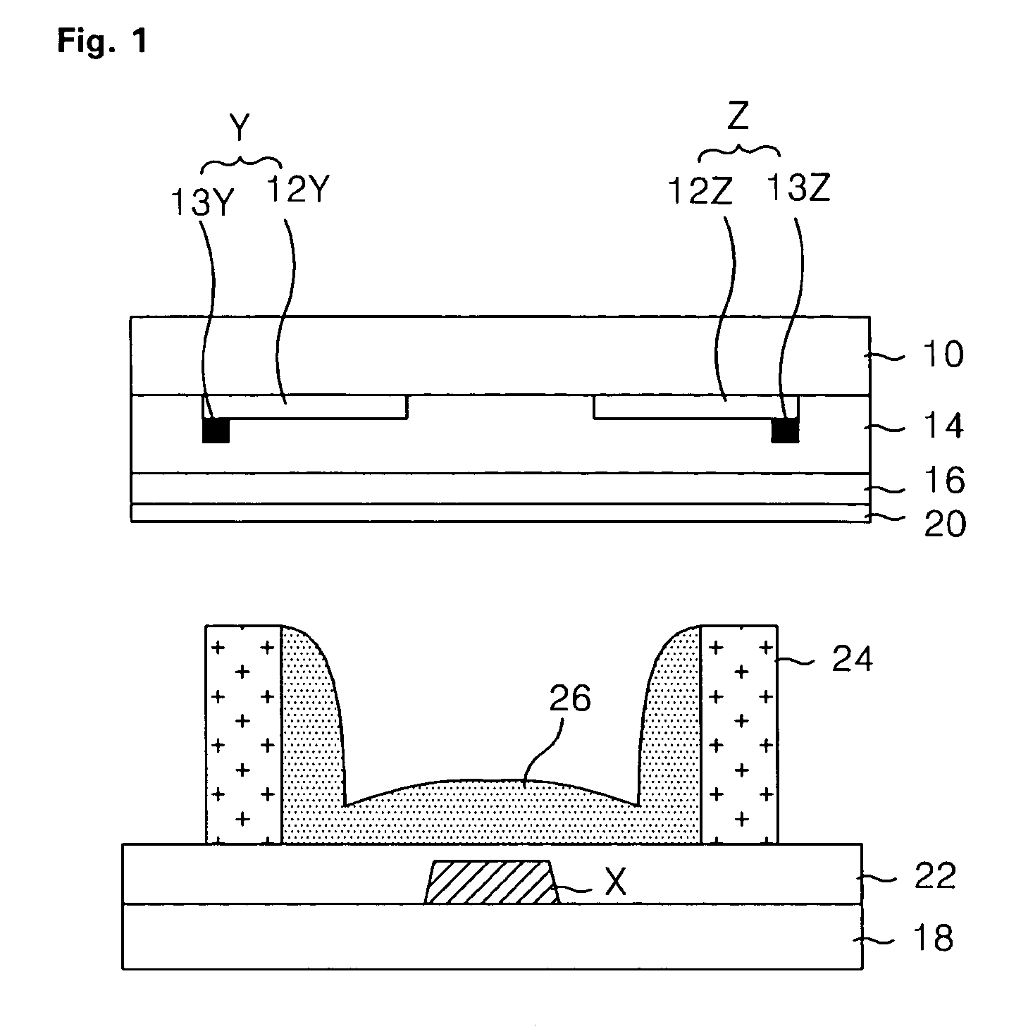
[0022] According to a first embodiment of the present invention, a plasma display panel including a plurality of a pair of display electrodes formed and arranged parallely on an upper plate, a plurality of address electrodes formed on a lower plate and arranged to be crossed to the display electrodes, a barrier rib defined a discharge space on the lower plate, and fluorescent body formed between the barrier ribs, includes further: a number of discharge cells having the discharge space; and an alkali metal layer formed in the discharge cells for supplying electrons to the discharge space.

[0023] Further, each of the discharge cells comprises a protection film, and the alkali metal layer is formed on the protection film.

[0024] Further, each of the discharge cells comprises an upper dielectric layer and a protection film, and the alkali metal layer is formed between the upper dielectric layer and the protection film.

[0025] Further, the alkali metal layer has a thickness of 5 Å to 100...

second embodiment

[0060] According to a second embodiment of the present invention, a plasma display panel including a plurality of a pair of display electrodes formed and arranged parallely on an upper plate, a plurality of address electrodes formed on a lower plate and arranged to be crossed to the display electrodes, a barrier rib defined a discharge space on the lower plate, and fluorescent body formed between the barrier ribs, wherein the plasma display panel includes further: a number of discharge cells having the discharge space; and an alkali metal layer formed in each of the discharge cells for supplying electrons to the discharge spaces, and a concentration of Xe in the discharge space is 10% or more.

[0061]FIG. 4 is a cross-sectional view illustrating a plasma display panel according to a second embodiment of the present invention.

[0062] A discharge cell of the PDP shown in FIG. 4 includes a pair of sustain electrodes formed on an upper substrate 10, i.e., a scan electrode Y and a sustain...


PUM


Abstract

The present invention relates to a plasma display panel and method for manufacturing the same in which electron discharge characteristic is improved and a voltage margin can be secured. According to a first embodiment of the present invention, a plasma display panel including a plurality of a pair of display electrodes formed and arranged parallely on an upper plate, a plurality of address electrodes formed on a lower plate and arranged to be crossed to the display electrodes, a barrier rib defined a discharge space on the lower plate, and fluorescent body formed between the barrier ribs, includes further: a number of discharge cells having the discharge space; and an alkali metal layer formed in the discharge cells for supplying electrons to the discharge space.

Description

CROSS-REFERENCE TO RELATED APPLICATIONS [0001] This Nonprovisional application claims priority under 35 U.S.C. § 119(a) on patent application No. 10-2003-0064811 filed in Korea on Sep. 18, 2003 and application No. 10-2004-0072647 filed in Korea on Sep. 08, 2004, the entire contents of which are hereby incorporated by reference. [0002] 1. Field of the Invention [0003] The present invention relates to a plasma display panel, and more particularly, to a plasma display panel and method for manufacturing the same in which electron discharge characteristic is improved and a voltage margin can be secured. [0004] 2. Background of the Related Art [0005] A plasma display panel (hereinafter, referred to as a ‘PDP’) is adapted to display an image including characters or graphics by light-emitting phosphors with ultraviolet of 147 nm generated during the discharge of an inert mixed gas such as He+Xe, Ne+Xe or He+Ne+Xe., This PDP can be easily made thin and large, and it can provide greatly incre...

Claims


Application Information

Patent Timeline
IPC IPC(8): H01J11/12H01J9/02H01J11/22H01J11/24H01J11/26H01J11/34H01J11/40H01J11/50
CPCH01J11/40H01J11/12
Inventor LEE, SANG KOOKKIM, JOONG KYUN
Owner LG ELECTRONICS INC
Why Eureka
Try Eureka