Nanoscale electronic devices & frabrication methods

a technology of electronic devices and nano-scale structures, applied in the direction of nanoinformatics, conductors, insulating supports, etc., can solve the problems of long time periods, difficult, and expensive to assemble building blocks, and prevent widespread commercial us

Inactive Publication Date: 2005-03-24
UNIVERSITY OF CANTERBURY
View PDF11 Cites 154 Cited by
  • Summary
  • Abstract
  • Description
  • Claims
  • Application Information

AI Technical Summary

Benefits of technology

In one preferred embodiment the step of formation of the chain of conducting nanoparticles is step i., and the geometry of the contacts in relation to each other and in relation to nanoparticle size has been optimised so as to increase the likelihood of the formation of a chain of nanoparticles at a surface coverage where conduction would not normally be expected in a macroscopic film or part thereof, of the same particles.
Preferably the nanowire structure is encapsulated in an insulating or dielectric material which protects it from oxidisation and allows the fabrication of a third contact, isolated from the nanowire, and which can therefore act as a gate.

Problems solved by technology

One of the challenges in this field is to develop nanostructured devices that will take advantage of the laws of quantum physics.
The challenge now is to translate these same device concepts into structures with dimensions of only a few nanometres, since the full range of quantum effects and novel device functionalities could then be available at room temperature.
However, as is also discussed below, there remain many challenges to overcome before such devices find commercial applications.
The ‘bottom-up’ approach proposes the assembly of devices from nanoscale building blocks, thus immediately achieving nanoscale resolution, but the approach usually suffers from a range of other problems, including the difficulty, expense, and long time periods that can be required to assemble the building blocks.
However, the difficulty in isolating and manipulating single nanotubes to form reproducible devices may prevent widespread commercial usage.
Hence the development of new techniques for the formation of nanoscale wire structures between electrically conducting contacts is an important technological problem.
This technique, while interesting, is not well suited to device formation since generally the technique is difficult to control, only a single wire can be fabricated at any time, and since multi-terminal devices cannot be easily achieved.
This approach is promising because the width of the wire is controlled by the size of the clusters, but the problem of positioning the clusters to form real devices on useful substrates has yet to be solved.
These devices are potentially very powerful but, equally, are most likely to be subject to difficulties associated with the expense and long time periods that can be required to assemble the building blocks.
Device to device reproducibility, and difficulty of positioning of the nanoparticles may be additional problems.
In some cases the use of a scanning tunnelling microscope leads to a slow and not scalable fabrication process.
While this is a significant achievement, and an element of self assembly in the fabrication is attractive, such devices are still far from commercial production and the methods used may not be viable for large scale production.
While these techniques may still be important in the future, the limitations include the limited range of types of nanoparticles that can be formed using these techniques, the difficulty in coding specific sites to attract nanoparticles, and there are so far unanswered questions regarding their suitability for scaling.

Method used


Image

  • Nanoscale electronic devices & frabrication methods
  • Nanoscale electronic devices & frabrication methods
  • Nanoscale electronic devices & frabrication methods

Examples


examples

The invention is further illustrated by the following examples:

1. Lithography Processes

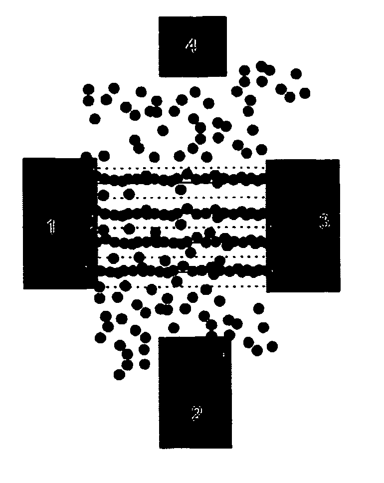
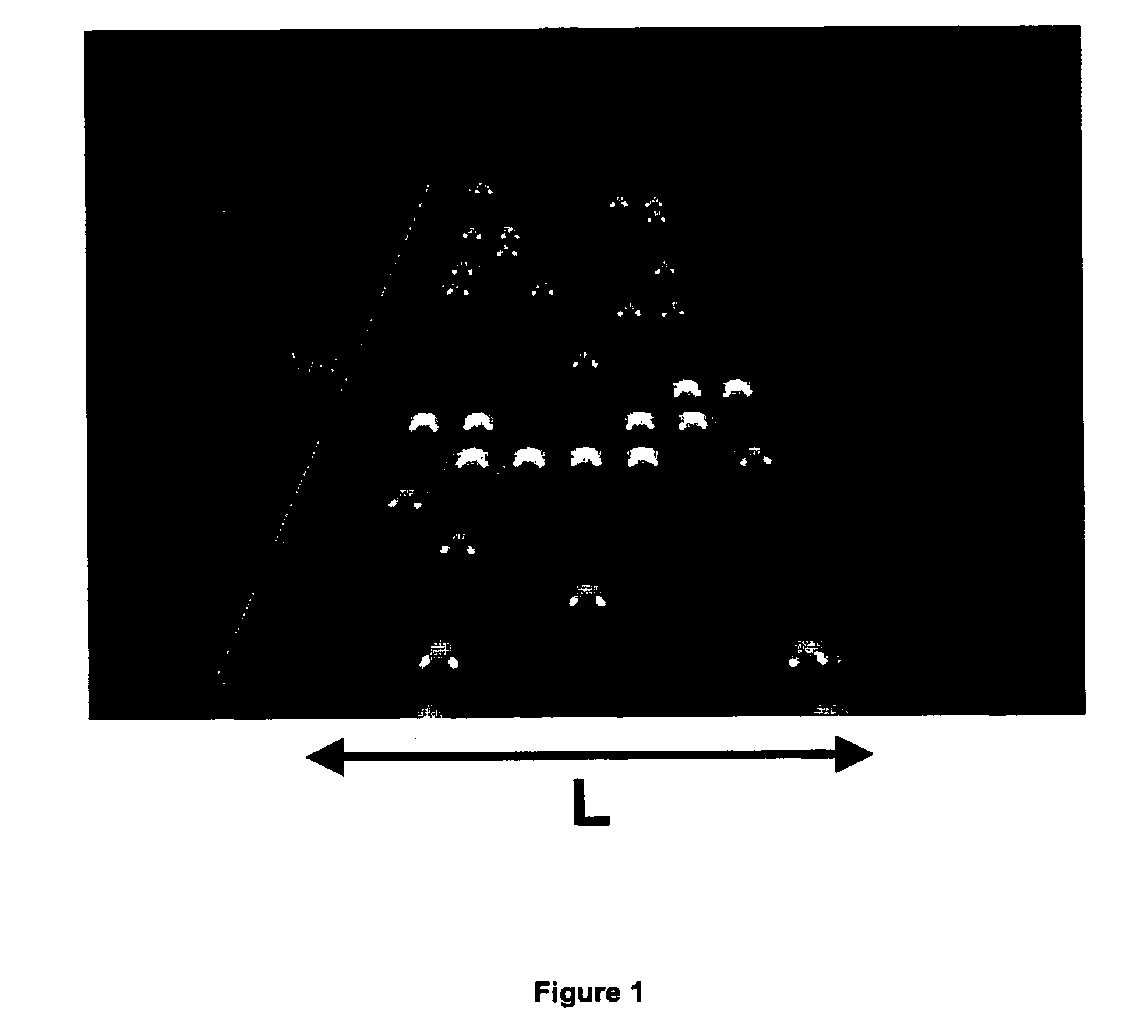
A combination of optical and Electron Beam Lithography has been used. The first technique defines macroscopic bonding pads with a moderate separation of about 40 microns. Subsequently, EBL defines the fine structure of the two contacts. For optical microscope pictures of fabricated contacts see FIG. 4.

(a) Cleaving and Cleaning of the Substrate

The substrates for the contacts are flat, square silicon pieces cut out of a standard 0.55 mm thick wafer with a 200 nm Silicon-nitride layer on top to provide a virtually non-conducting and very flat surface.

After cutting the wafer into pieces of the required size, the substrates are cleaned. That is achieved by rinsing them first in Acetone then Methanol and finally IPA making intensive use of the ultrasonic bath. After the IPA the substrates are blown dry with N2 and baked at 95 degrees Celsius for about 15 minutes before further processing.

(b...


PUM

PropertyMeasurementUnit
distanceaaaaaaaaaa
distanceaaaaaaaaaa
distanceaaaaaaaaaa

Abstract

The invention relates to a method of forming a conducting nanowire between two contacts on a substrate surface wherein a plurality of nanoparticles is deposited on the substrate in the region between the contacts, and the single nanowire running substantially between the two contacts is formed by either by monitoring the conduction between the contacts and ceasing deposition at the onset of conduction, and / or modifying the substrate to achieve, or taking advantage of pre-existing topographical features which will cause the nanoparticles to form the nanowire. The resultant conducting nanowires are also claimed as well as devices incorporating such nanowires.

Description

FIELD OF THE INVENTION The present invention relates to methods of preparing electrically conducting nanoscale wire-like structures for use in electronic devices and the devices formed by such methods. More particularly but not exclusively the invention relates to a method of preparing such structures by the assembly of conducting nanoparticles. BACKGROUND TO THE INVENTION Nanotechnology has been identified as a key technology for the 21st century. This technology is centred on an ability to fabricate electronic, optical and opto-electronic devices on the scale of a few billionths of a metre. In the future, such devices will underpin new computing and communications technologies and will be incorporated in a vast array of consumer goods. There are many advantages of fabricating nanoscale devices. In the simplest case, such devices are much smaller than the current commercial devices (such as the transistors used in integrated circuits) and so provide opportunities for increased p...

Claims


Application Information

Patent Timeline
Patent Type & Authority Applications(United States)
IPC IPC(8): H01B5/00B82B3/00H01B5/14H01B13/00H01L29/06H01L29/76H01L49/00
CPCB82Y10/00H01L29/7613Y10S977/72Y10S977/773H01L49/006H10N99/05B82B3/00B82Y40/00
Inventor BROWN, SIMON ANTHONYSCHMELZER, JUERN
Owner UNIVERSITY OF CANTERBURY
Why Eureka
Try Eureka