Low noise vertical variable gate control voltage JFET device in a BiCMOS process and methods to build this device

Active Publication Date: 2005-03-31
TEXAS INSTR INC
View PDF3 Cites 20 Cited by
  • Summary
  • Abstract
  • Description
  • Claims
  • Application Information

AI Technical Summary

Problems solved by technology

One dominant noise source in a transistor is the interaction of the mobile charge carriers and crystal imperfections in the device.

Method used


Image

  • Low noise vertical variable gate control voltage JFET device in a BiCMOS process and methods to build this device
  • Low noise vertical variable gate control voltage JFET device in a BiCMOS process and methods to build this device
  • Low noise vertical variable gate control voltage JFET device in a BiCMOS process and methods to build this device

Examples


Embodiment Construction

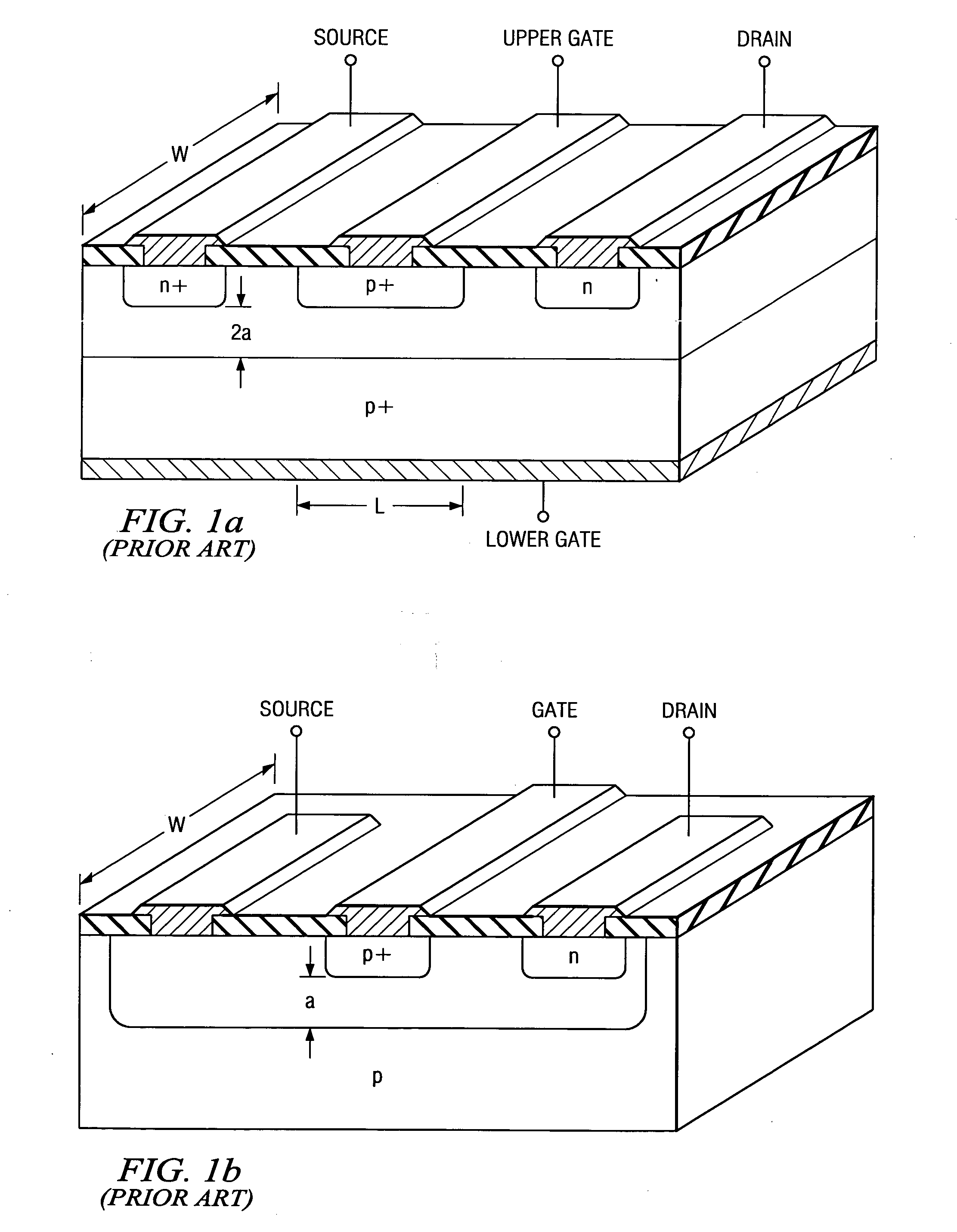
Applicants recognize that, due to traditional wafer processing, the top surface of a semiconductor substrate is usually heavily populated with imperfections such as dangling bonds and charge traps. Interactions between the mobile charge carriers in the substrate and the surface imperfections limit the performance of semiconductor devices in which the current flows parallel and close to the top surface of the substrate. This invention meliorate the limitations by forming a device that has a “vertical” channel, that is, a channel that runs substantially perpendicular to the top surface of the substrate and in which the current flows substantially away from the top surface of the substrate.

In this configuration, the interaction between the charge carrier and the surface imperfection is substantially reduced, which enables the device to have superior cutoff frequency (fco) and 1 / f noise figure.

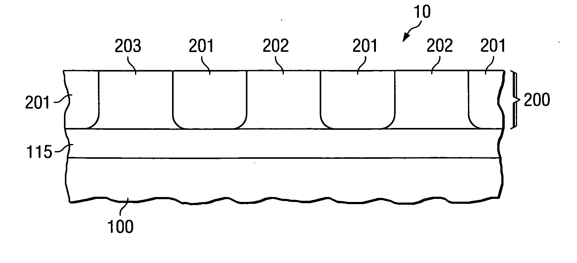
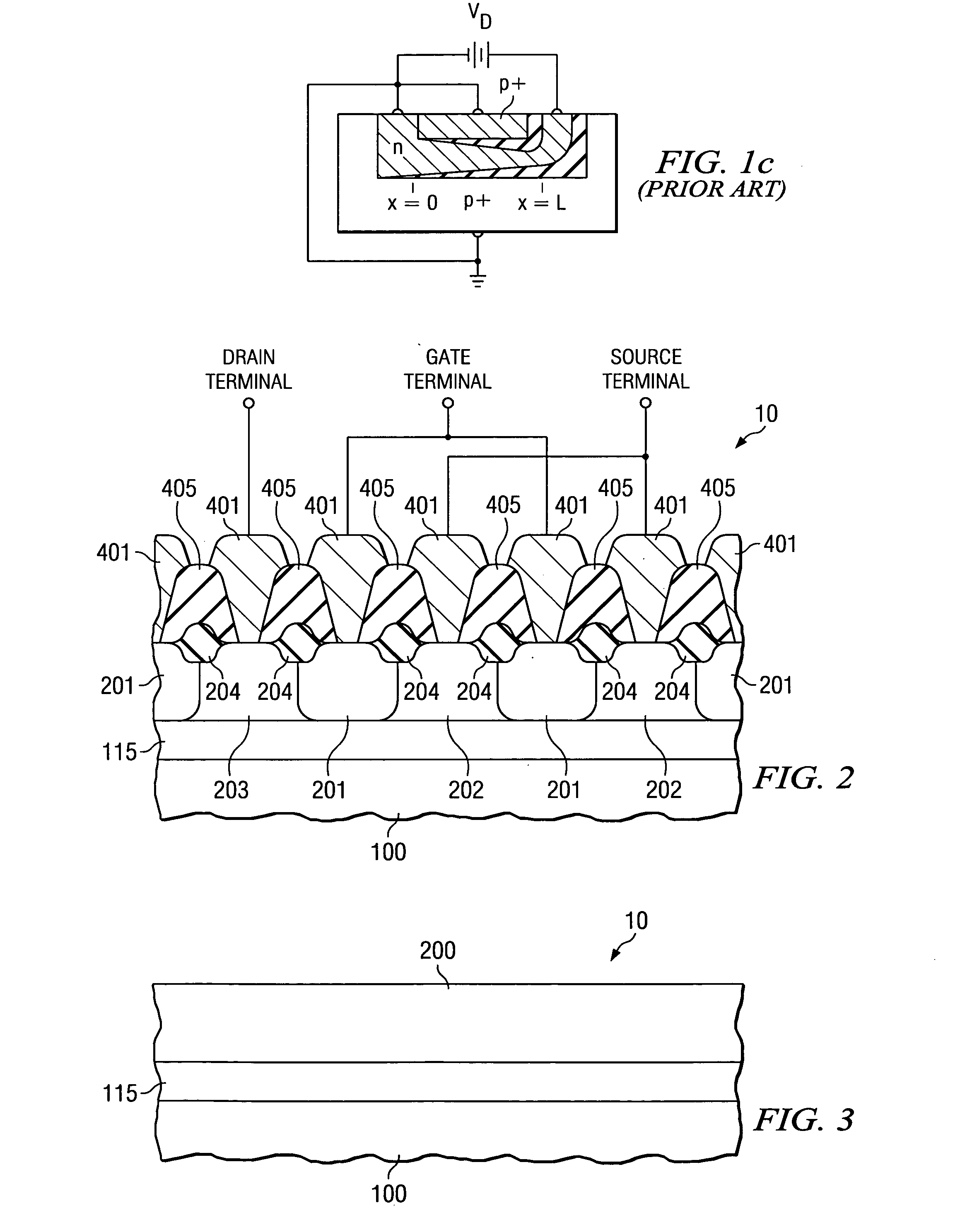
FIG. 2 depicts a partial sectional depiction of a semiconductor substrate with a JFET embo...


PUM


Abstract

We disclose the structure of a JFET device, the method of making the device and the operation of the device. The device is built near the top of a substrate. It has a buried layer that is electrically communicable to a drain terminal. It has a channel region over the buried layer contacting gate regions that connect to a gate terminal. The channel region, of which the length spans the distance between the buried layer and a source region, is connected to a source terminal. The device current flows in the channel substantially perpendicularly to the top surface of the substrate.

Description

BACKGROUND OF THE INVENTION This invention relates to semiconductor devices and particularly to an improved junction field effect transistor (JFET). A conventional JFET is a three-terminal semiconductor device in which a current flows substantially parallel to the top surface of the semiconductor chip and the flow is controlled by a vertical electric field, as shown in FIGS. 1a, 1b, and 1c. It can be used as a current switch or a signal amplifier. JFETs are known as unipolar transistors because the current is transported by carriers of one polarity, namely, the majority carriers. This is in contrast with bipolar junction transistor, in which both majority-and-minority-carrier currents are important. A typical n-channel JFET fabricated by the standard planar process is shown in FIG. 1. FIG. 1a depicts an n-channel JFET of which the channel is a part of an epitaxial semiconductor layer. FIG. 1b depicts another n-channel JFET of which the channel is formed with a double-diffusion t...

Claims


Application Information

Patent Timeline
Patent Type & Authority Applications(United States)
IPC IPC(8): H01L21/337H01L21/8249H01L27/06H01L29/10H01L29/808
CPCH01L21/8249H01L27/0623H01L29/808H01L29/66901H01L29/1066
Inventor PENDHARKER, SAMEER P.HAO, PINGHAIWU, XIAOJU
Owner TEXAS INSTR INC
Why Eureka
Try Eureka