Semiconductor device and method for fabricating the same

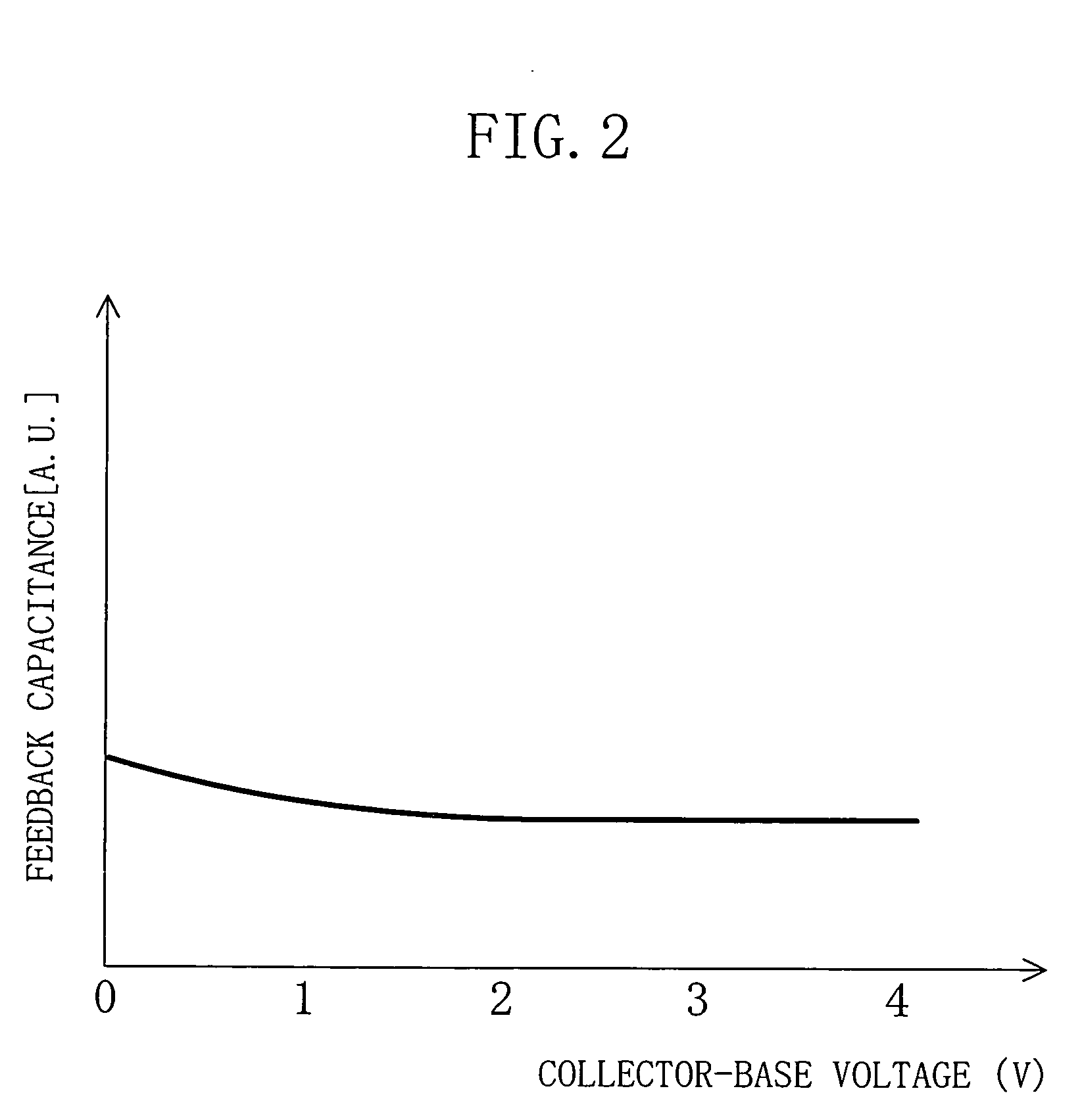
a technology of semiconductor devices and semiconductor substrates, applied in semiconductor devices, semiconductor/solid-state device details, electrical apparatus, etc., can solve the problems of different substrates of silicon substrates from regular silicon substrates, increased costs, and inability to use them in fabrication. to prevent the fluctuation of feedback capacitan

Active Publication Date: 2005-03-31
PANNOVA SEMIC
View PDF4 Cites 6 Cited by
  • Summary
  • Abstract
  • Description
  • Claims
  • Application Information

AI Technical Summary

Benefits of technology

[0012] It is therefore an object of the present invention to solve the above-described known problems and prevent fluctu...

Problems solved by technology

However, the SOI substrate is different from a regular silicon substrate and very special and costs are i...

Method used


Image

  • Semiconductor device and method for fabricating the same
  • Semiconductor device and method for fabricating the same
  • Semiconductor device and method for fabricating the same

Examples


first embodiment

Modified Example of First Embodiment

[0048] Hereinafter, a modified example of the first embodiment of the present invention will be described with reference to the accompanying drawings.

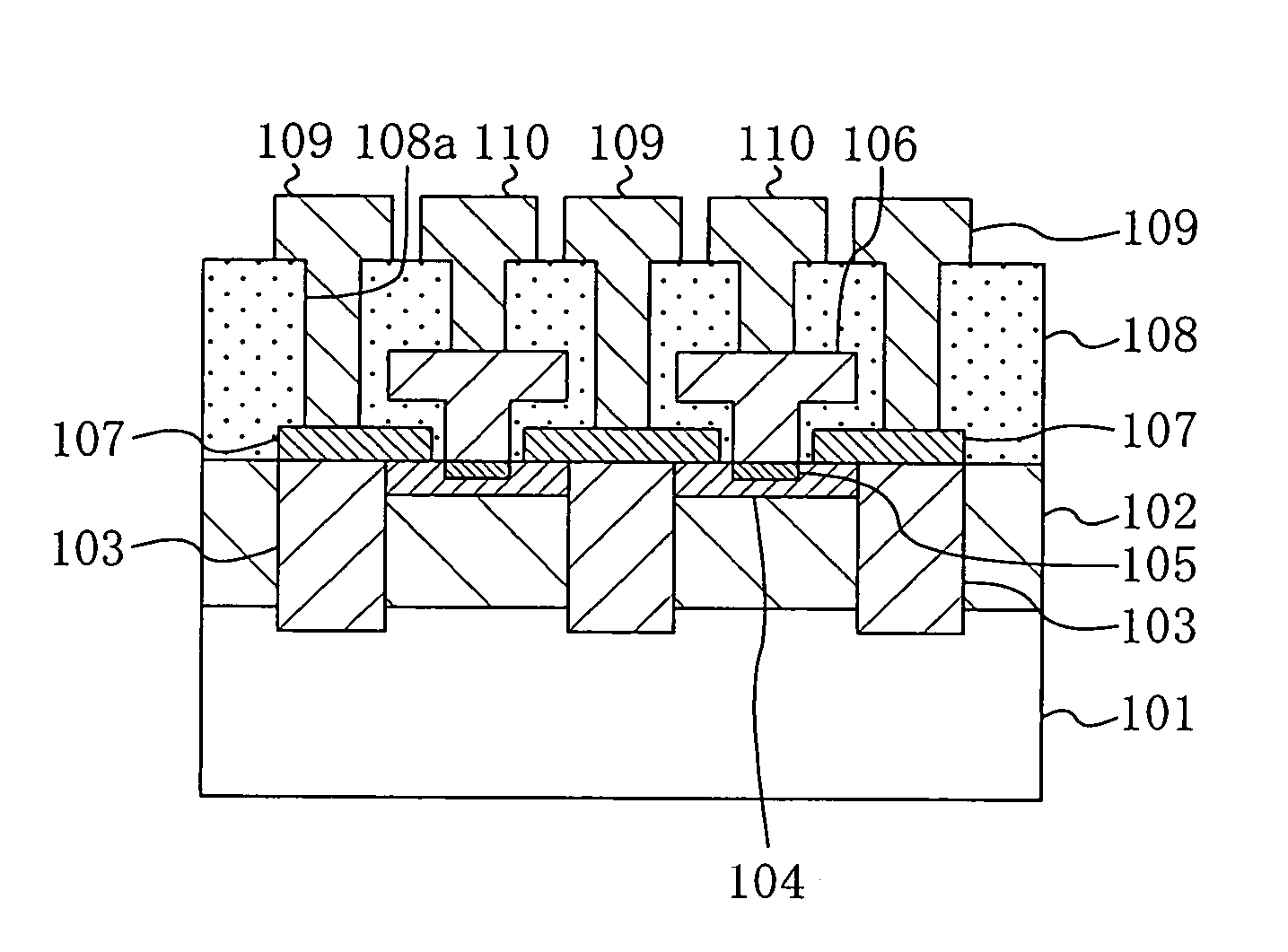
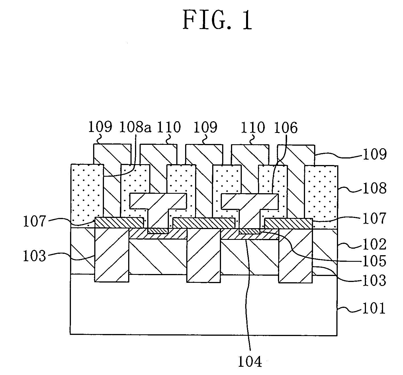
[0049]FIG. 3 is a cross-sectional view illustrating a semiconductor device according to the modified example of the first embodiment of the present invention. In FIG. 3, each member also shown in FIG. 1 is identified by the same reference numeral and therefore the description thereof will be omitted.

[0050] As shown in FIG. 3, in this modified embodiment, an intrinsic base region 204 is formed on a collector layer 102 by selective epitaxial growth.

[0051] Hereinafter, a method for fabricating the semiconductor device of this modified example configured in the above-described manner will be described with reference to FIGS. 4A through 4E and FIGS. 5A through 5D.

[0052] First, as shown in FIG. 4A, on an n-type semiconductor substrate 101 made of a silicon (Si) single crystal doped with arsenic (As) so...

second embodiment

Modified Example of Second Embodiment

[0082] Hereinafter, a modified example of the second embodiment of the present invention will be described with reference to the accompanying drawings.

[0083]FIG. 10 is a cross-sectional view illustrating a semiconductor device according to the modified example of the second embodiment of the present invention. In FIG. 10, each member also shown in FIG. 6 is identified by the same reference numeral and therefore the description thereof will be omitted.

[0084] As shown in FIG. 10, in this modified embodiment, an intrinsic base region 404 is formed on part of the collector layer 302 located in the inner side than each of the insulating trenches 312 by selective epitaxial growth. Note that the intrinsic base region 404 formed by epitaxial growth can be formed in the same manner as in FIG. 4C of the modified example of the first embodiment.

[0085] Note that in each of the modified examples of the first and second embodiments, description has been mad...


PUM


Abstract

A semiconductor device includes a semiconductor substrate of a first conductive type, a collector layer formed on the semiconductor substrate and made of a first semiconductor being of the first conductive type and having a higher resistance than that of the semiconductor substrate, an intrinsic base region having a junction surface with the collector layer and made of a second semiconductor of a second conductive type, and an emitter region having a junction surface with the intrinsic base region and made of a third semiconductor of the first conductive type. A periphery of the intrinsic base region is surrounded by an insulating region extending from the collector layer to the semiconductor substrate.

Description

CROSS-REFERENCE TO RELATED APPLICATION [0001] The disclosure of Japanese Patent Application No. 2003-333388 filed on Sep. 25, 2003 including specification, drawings and claims is incorporated herein by reference in its entity. BACKGROUND OF THE INVENTION [0002] The present invention relates to bipolar transistors and more particularly relates to a semiconductor device including a bipolar transistor having a substrate itself serving as an electrode. [0003] Semiconductor devices have a configuration in which many active devices can be integrated on a semiconductor substrate. However, in a high frequency device for use in a cellular phone, a device is required to have high performance and a small variation in electrical characteristics and, therefore, a discrete semiconductor element such as an elemental bipolar transistor is used in many cases. Specifically, in a VCO (voltage-controlled oscillator) device required to have a breakdown voltage of 5 V or more at a power supply voltage of...

Claims


Application Information

Patent Timeline
IPC IPC(8): H01L21/331H01L21/8222H01L27/082H01L29/06H01L29/08H01L29/10H01L29/417H01L29/423H01L29/732
CPCH01L21/8222H01L27/0823H01L29/0649H01L29/0821H01L29/732H01L29/41708H01L29/42304H01L29/66272H01L29/1004
Inventor TOYODA, YASUYUKISONETAKA, SHINICHI
Owner PANNOVA SEMIC
Why Eureka
Try Eureka