

Semiconductor device and manufacturing method thereof
- Summary
- Abstract
- Description
- Claims
- Application Information
AI Technical Summary
Benefits of technology
Problems solved by technology
Method used
Image

Examples
first embodiment
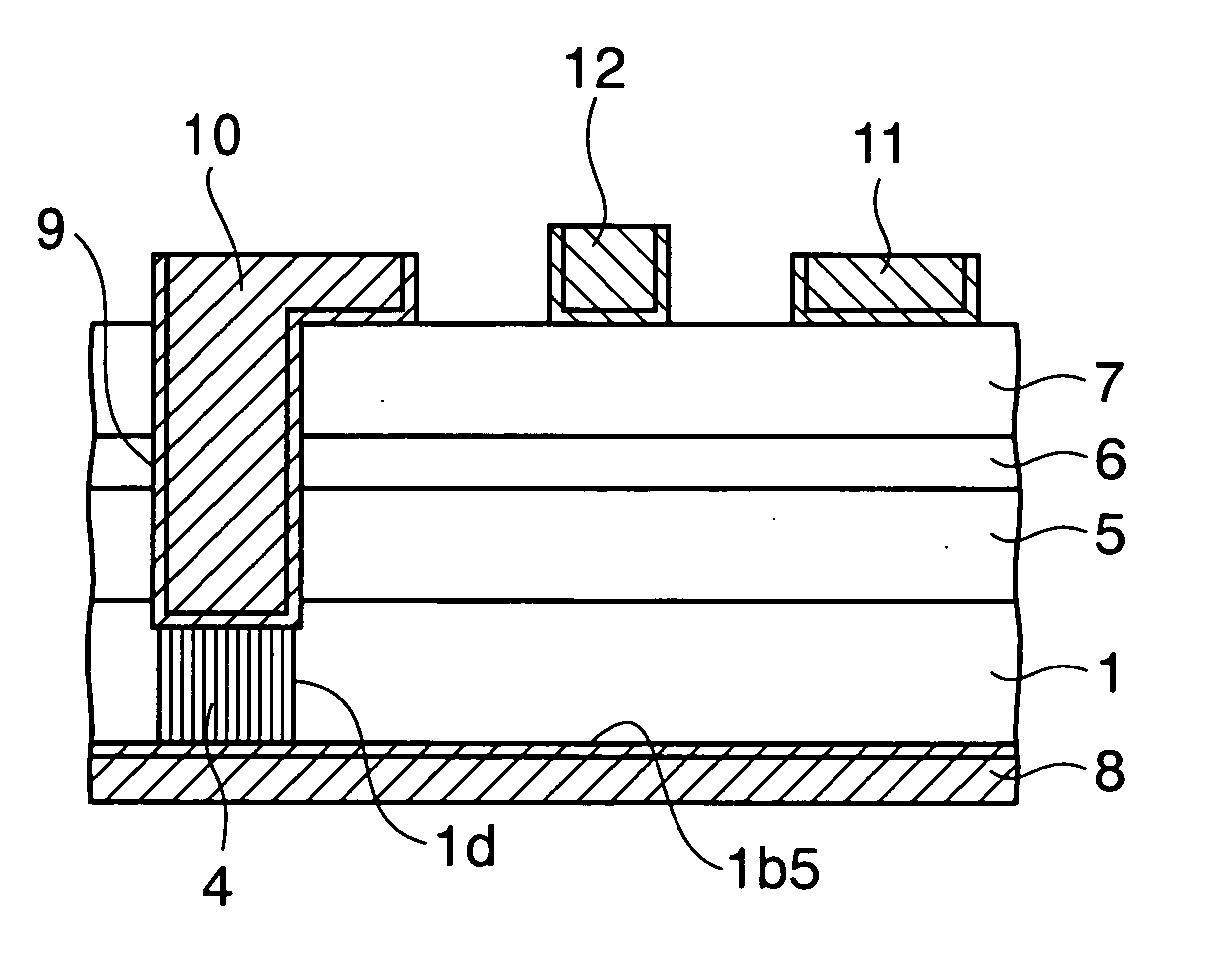
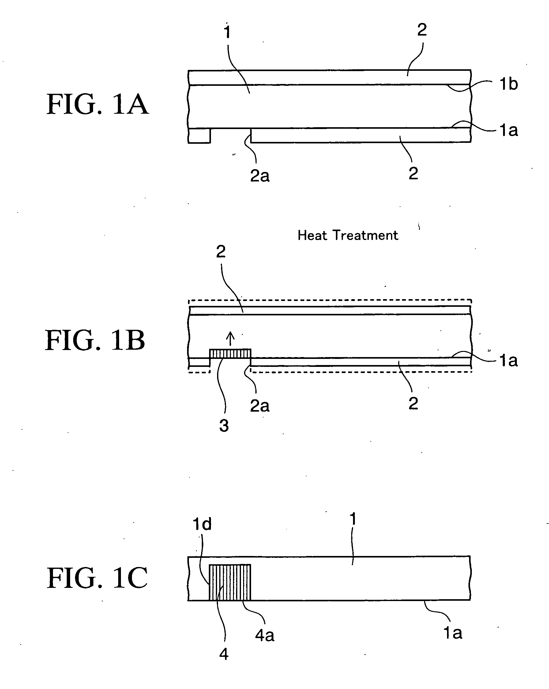
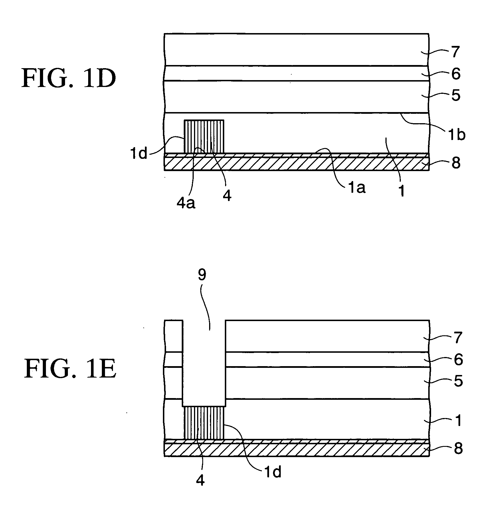
[0047]FIGS. 1A to 1G are cross-sectional views showing a method of manufacturing a semiconductor device according to a first embodiment of the present invention in order of processes.
[0048] In this embodiment, an AlGaN / GaN heterojunction HEMT is fabricated as an example of the semiconductor device.
[0049] First, a process until obtaining a cross-sectional structure shown in FIG. 1A will be described.
[0050] First, silicon nitride films are formed as a mask film 2 to a thickness of approximately 500 nm by a plasma CVD method on a surface 1a and the other surface 1b of a SiC substrate 1 whose thickness is thinned to approximately 100 μm. Thereafter, a resist pattern (not shown) is formed on one of the mask films 2. While using the resist pattern as a mask, the mask film 2 on the surface 1a of the SiC substrate 1 is etched by dry etching using a fluorine-based etching gas such as SF6 gas, thus forming a window 2a. After that, the resist pattern is removed.
[0051] Subsequently, as show...
second embodiment
[0077]FIGS. 3A to 3D are cross-sectional views showing a method of manufacturing a semiconductor device according to a second embodiment of the present invention in order of processes. In these drawings, the same reference numerals as those in the first embodiment will be used to the members described in the first embodiment, and description thereof will be omitted below.
[0078] First, a process until obtaining a cross-sectional structure shown in FIG. 3A will be described.
[0079] First, the deposition method of the mask films 2, which has been described in the first embodiment, is employed, and silicon nitride films as first mask films 13 are formed to a thickness of approximately 500 nm by a CVD method on the respective surfaces 1a and 1b of the SiC substrate 1. Thereafter, a first window 13a is formed in the first mask film 13 on the surface 1a of the SiC substrate 1.
[0080] After that, a first heat treatment in which a substrate temperature is maintained at 1200 to 2000° C., and...
third embodiment
[0092]FIGS. 6A to 6C are cross-sectional views of a method of manufacturing a semiconductor device according to a third embodiment of the present invention. In these drawings, the same reference numerals will be used to the members already described in the first and second embodiments, and description thereof will be omitted below.
[0093] First, as shown in FIG. 6A, the first heat treatment described in the second embodiment is performed for the SiC substrate 1, and thus a first heat conductor 17a constructed from carbon nanotubes is formed in the surface 1a of the SiC substrate 1. Thereafter, a silicon nitride film is formed as the second mask film 15 to a thickness of 500 nm by a plasma CVD method and the like only on the other surface 1b of the SiC substrate 1.
[0094] Next, as shown in FIG. 6B, the second heat treatment described in the second embodiment is performed for the SiC substrate 1, and the carbon nanotubes are grown over the surface 1a of the SiC substrate 1, which is n...
PUM
 Abstract
Description
Claims
Application Information