Semiconductor integrated circuit device

a technology of integrated circuits and semiconductors, applied in semiconductor devices, digital storage, instruments, etc., can solve the problems of increasing current consumption, difficult to fabricate a dram cell composed of a conventional type, and inability to accurately discriminate data “1” and “0”

Inactive Publication Date: 2005-03-31
KK TOSHIBA
View PDF6 Cites 45 Cited by
  • Summary
  • Abstract
  • Description
  • Claims
  • Application Information

AI Technical Summary

Problems solved by technology

It may become difficult to fabricate a DRAM cell composed of a conventional one transistor and a trench capacitor or a stacked capacitor, as the DRAM cell becomes finer.
Therefore, the data “1” and “0” cannot be discriminated accurately.
This results in a problem that current consumption increases.
In addition, as a major problem, unbalance in capacitance between the bit line and the reference bit line cannot be avoided and it becomes impossible in the dynamic sense scheme to sense data normally, if the reference cell for data “1” and the reference cell for data “0” are provided.
However, there is a likelihood that the finer transistor technique will not be advanced unlike heretofore due to physical limits.

Method used


Image

  • Semiconductor integrated circuit device
  • Semiconductor integrated circuit device
  • Semiconductor integrated circuit device

Examples


first embodiment

[0063] (First Embodiment)

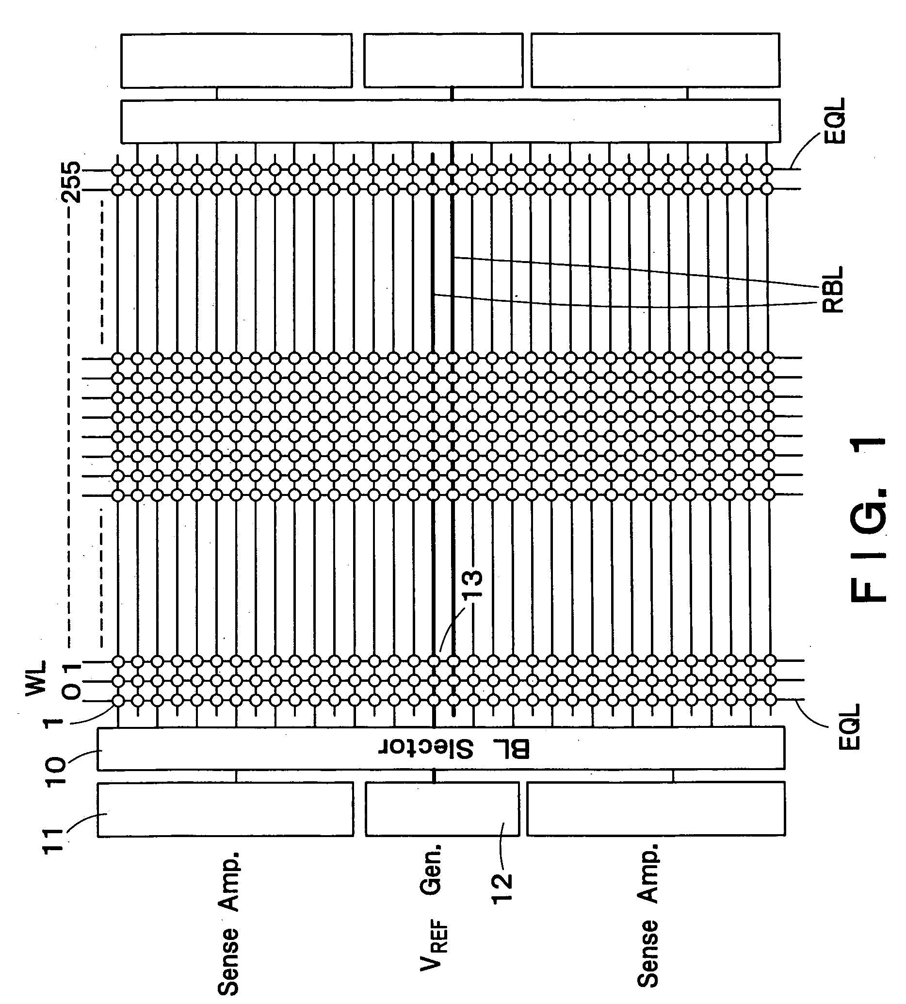
[0064]FIG. 1 is a block diagram showing a schematic configuration of a semiconductor integrated circuit device according to a first embodiment of the present invention. FIG. 1 is a diagram obtained by picking out 256 word lines WL and 32 bit lines BL. Although the whole of one array is shown in the direction of the word line WL, only a part of the one array is shown in the direction of the bit line BL. In practice, a collection that is 32 times as large as the 32 bit lines BL, i.e., a collection having a total of 1,024 bit lines BL forms one array. And a memory is composed of a plurality of arrays.

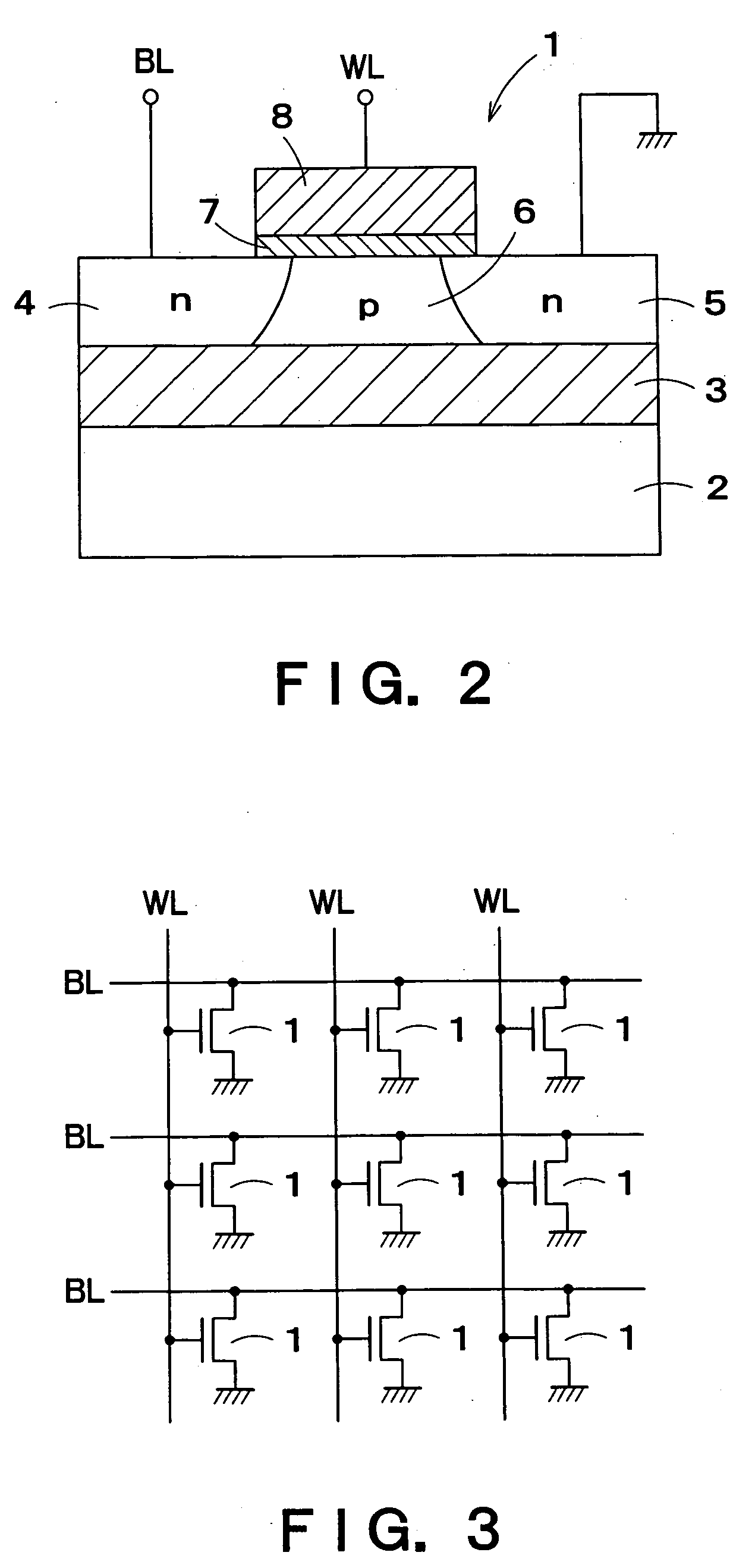
[0065] A DRAM cell 1 formed of an FBC is connected to each of intersections of the word lines WL and the bit lines BL. The DRAM cell 1 is formed of one MISFET having a floating channel body. FIG. 2 is a sectional view showing a structure of a DRAM cell 1 using an n-channel MISFET. An insulation film 3 such as a silicon oxide film is formed on a silicon substrate 2...

second embodiment

[0104] (Second Embodiment)

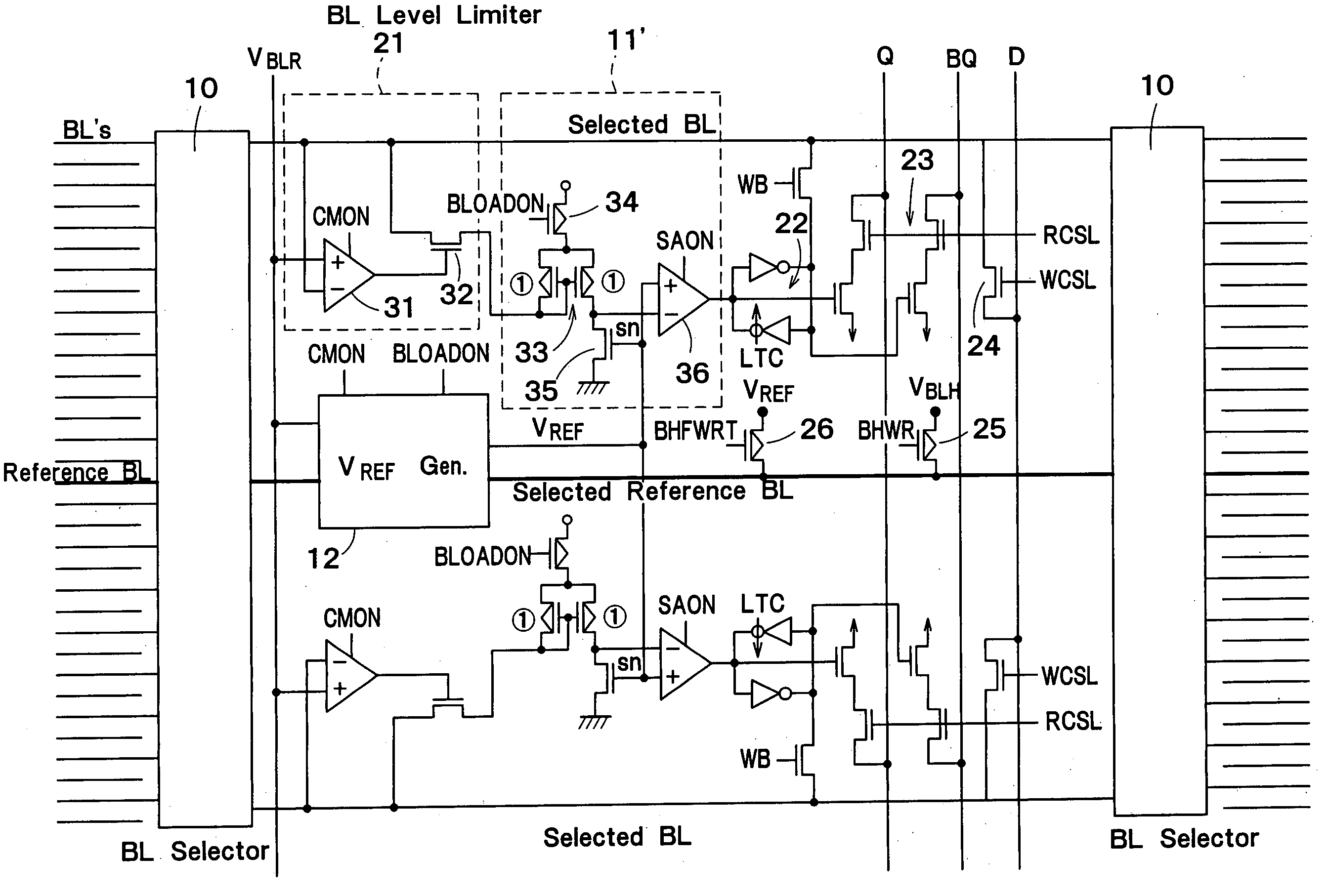
[0105] In a second embodiment, a dynamic sense amplifier 11 of voltage sense type is provided.

[0106]FIG. 11 is a circuit diagram according to a second embodiment of the sense amplifier block 11. In FIG. 11, components common to FIG. 8 are denoted by like characters, and hereafter different points will be mainly described.

[0107] The sense amplifier shown in FIG. 11 is a dynamic sense amplifier of voltage sense type. The sense amplifier includes a latch circuit 51 for latching a potential difference between an output node bsn of a level limiter 21 and an output node sn of a reference potential generator circuit 12, a p-FET 25 for conducting switching control to determine whether to set the reference bit line RBL to the “1” potential, a p-FET 26 for conducting switching control to determine whether to set the reference bit line RBL to the “½” potential, a write back control transistor 52, a read control circuit 23, and a write control circuit 24.

[0108] The ...

third embodiment

[0116] (Third Embodiment)

[0117] A third embodiment is a variant of the second embodiment.

[0118]FIG. 13 is a circuit diagram of a third embodiment of the sense amplifier block 11. In FIG. 13, components common to FIG. 11 are denoted by like characters, and hereafter different points will be mainly described.

[0119] The sense amplifier shown in FIG. 13 is the same as the circuit described in detail in T. N. Blalock and R. C. Jaeger, “A High-Speed Clamped Bit-Line Current-Mode Sense Amplifier,” IEEE J. Solid State Circuits, vol. 26, No.4, pp. 542-548, April 1991.

[0120] The sense amplifier shown in FIG. 13 is different in the configuration of the latch circuit 51 from the sense amplifier shown in FIG. 11. The latch circuit 51 shown in FIG. 13 includes a p-FET 63 and n-FETs 64 to 67 besides the p-FETs 53 and 54 and the n-FETs 55 and 56. The p-FET 53, n-FET 55 and n-FET 65 are connected in cascade. The p-FET 54, n-FET 56 and n-FET 66 are connected in cascade.

[0121] The output of the le...


PUM


Abstract

A semiconductor integrated circuit device, comprising: a semiconductor layer formed via an embedded insulation film on a substrate; an FBC (Floating Body Cell) which stores data by accumulating a majority carrier in a floating channel body formed on the semiconductor layer; a reference cell connected to a reference bit line, the reference cell having the same size, shape and electric properties as those of the FBC; an intermediate cell writing control circuit which performs control for writing intermediate potential which is less than data “1” and larger than data “0” in the channel body of the reference cell; and a sense amplifier which performs control for reading out data stored in a selected FBC based on the intermediate data read out from the reference cell.

Description

CROSS REFERENCE TO RELATED APPLICATIONS [0001] This application claims benefit of priority under 35 USC§119 to Japanese Patent Application No. 2003-341533, filed on Sep. 30, 2003, the entire contents of which are incorporated by reference herein. BACKGROUND OF THE INVENTION [0002] 1. Field of the Invention [0003] The present invention relates to a semiconductor integrated circuit device including a first semiconductor layer formed on a substrate via an embedded insulation film and an FBC (Floating Body Cell) for storing majority carriers in a floating channel body formed in the first semiconductor layer and thereby storing data. [0004] 2. Related Art [0005] It may become difficult to fabricate a DRAM cell composed of a conventional one transistor and a trench capacitor or a stacked capacitor, as the DRAM cell becomes finer. As a memory cell that can be used instead of such a DRAM cell, a new memory cell FBC that stores majority carriers in a floating body of an FET formed on a SOI (...

Claims


Application Information

Patent Timeline
Patent Type & Authority Applications(United States)
IPC IPC(8): G11C7/06G11C7/12G11C7/14H01L27/10G11C11/401G11C11/404G11C11/409G11C11/4091G11C11/4094G11C11/56H01L21/8242H01L27/108
CPCG11C7/062G11C7/12G11C7/14H01L29/7841G11C11/4094H01L27/108G11C11/4091H10B12/00
Inventor OHSAWA, TAKASHI
Owner KK TOSHIBA
Why Eureka
Try Eureka