

Method of forming mirrors by surface transformation of empty spaces in solid state materials
- Summary
- Abstract
- Description
- Claims
- Application Information
AI Technical Summary
Benefits of technology
Problems solved by technology
Method used
Image

Examples
Embodiment Construction
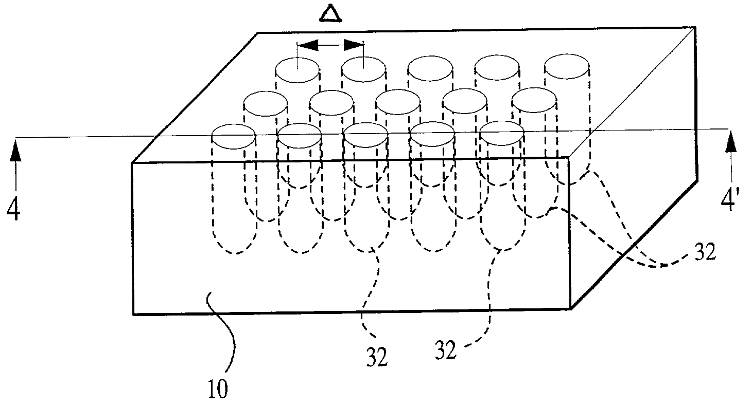
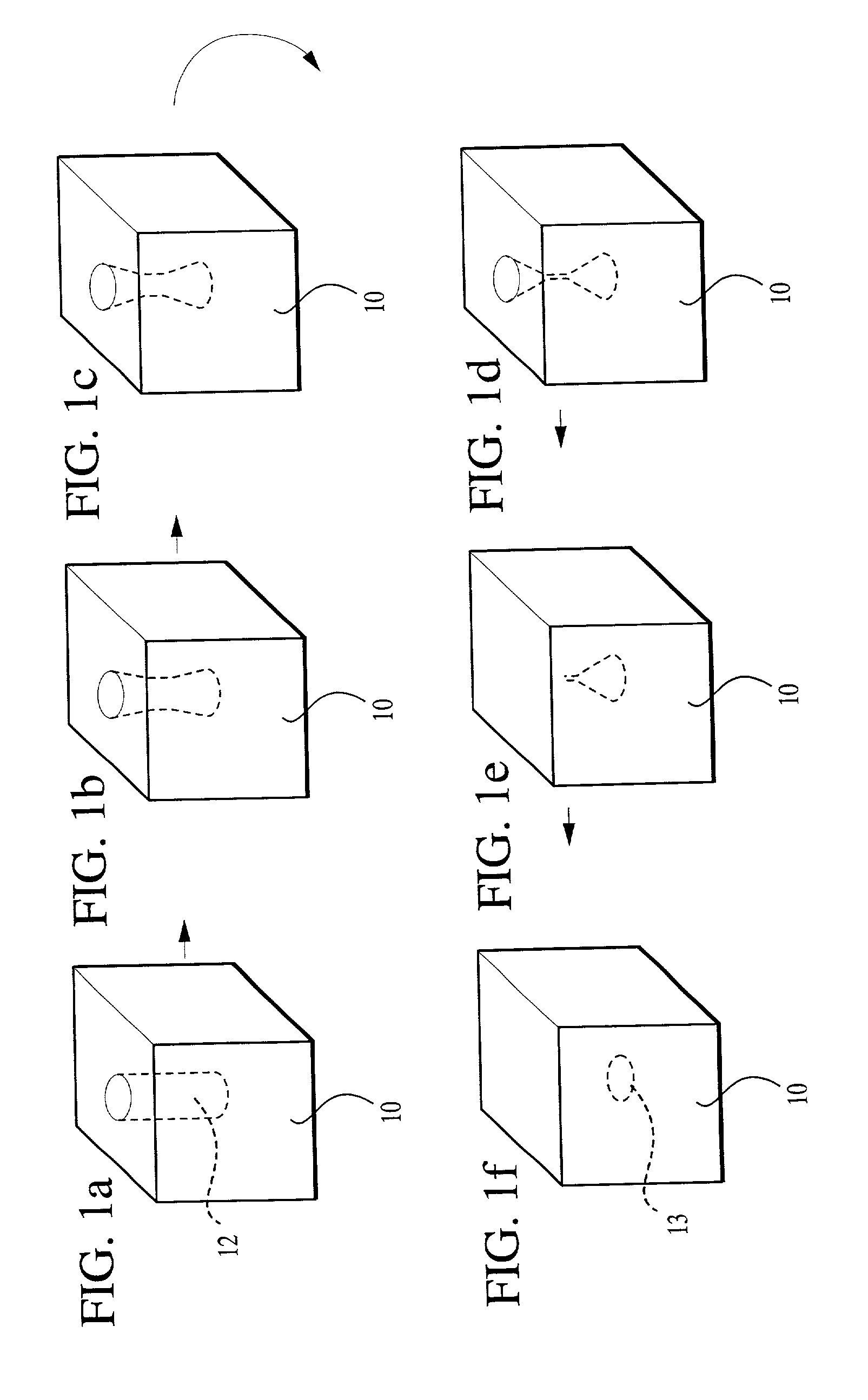
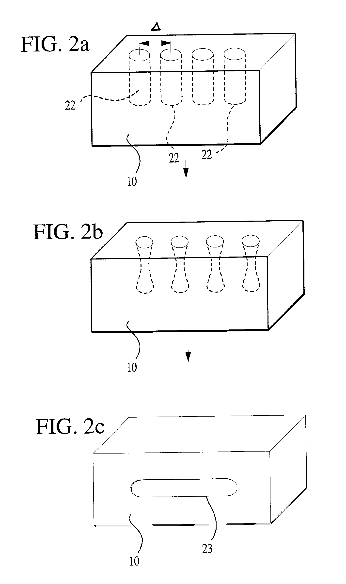
In the following detailed description, reference is made to various exemplary embodiments for carrying out the invention. These embodiments are described with sufficient detail to enable those skilled in the art to practice the invention, and it is to be understood that other embodiments may be employed, and that structural, electrical and process changes may be made, and equivalents substituted, without departing from the invention. Accordingly, the following detailed description is exemplary and the scope of the present invention is defined by the appended claims.
The term “substrate” used in the following description includes any light-transmissive material having a uniform structure and a reasonably defined melting temperature. The term “substrate” is to be understood as including substrates formed of silicon, quartz, glass, gallium arsenide, indium gallium arsenide, silicon-on-insulator, doped and undoped semiconductors, epitaxial layers of silicon supported by a base semicon...
PUM
 Abstract
Description
Claims
Application Information