Method of depositing high-quality sige on sige substrates

a technology of sige substrate and sige layer, which is applied in the direction of crystal growth process, electrical equipment, basic electric elements, etc., can solve the problem of reducing the performance of devices made from such layers

Inactive Publication Date: 2005-03-31
SIGE SEMICON
View PDF5 Cites 54 Cited by
  • Summary
  • Abstract
  • Description
  • Claims
  • Application Information

AI Technical Summary

Benefits of technology

[0015] Another advantage of using a thin Si seed layer is its compatibility with growth on patterned substrates. A thin Si seed layer

Problems solved by technology

As noted previously, above the critical thickness threading dislocations may be cre

Method used


Image

  • Method of depositing high-quality sige on sige substrates
  • Method of depositing high-quality sige on sige substrates

Examples


Embodiment Construction

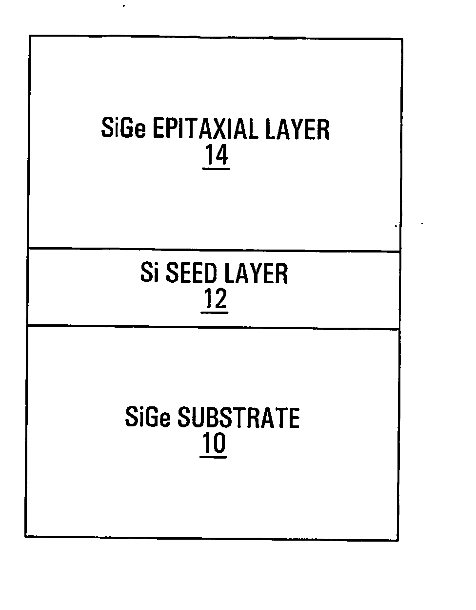
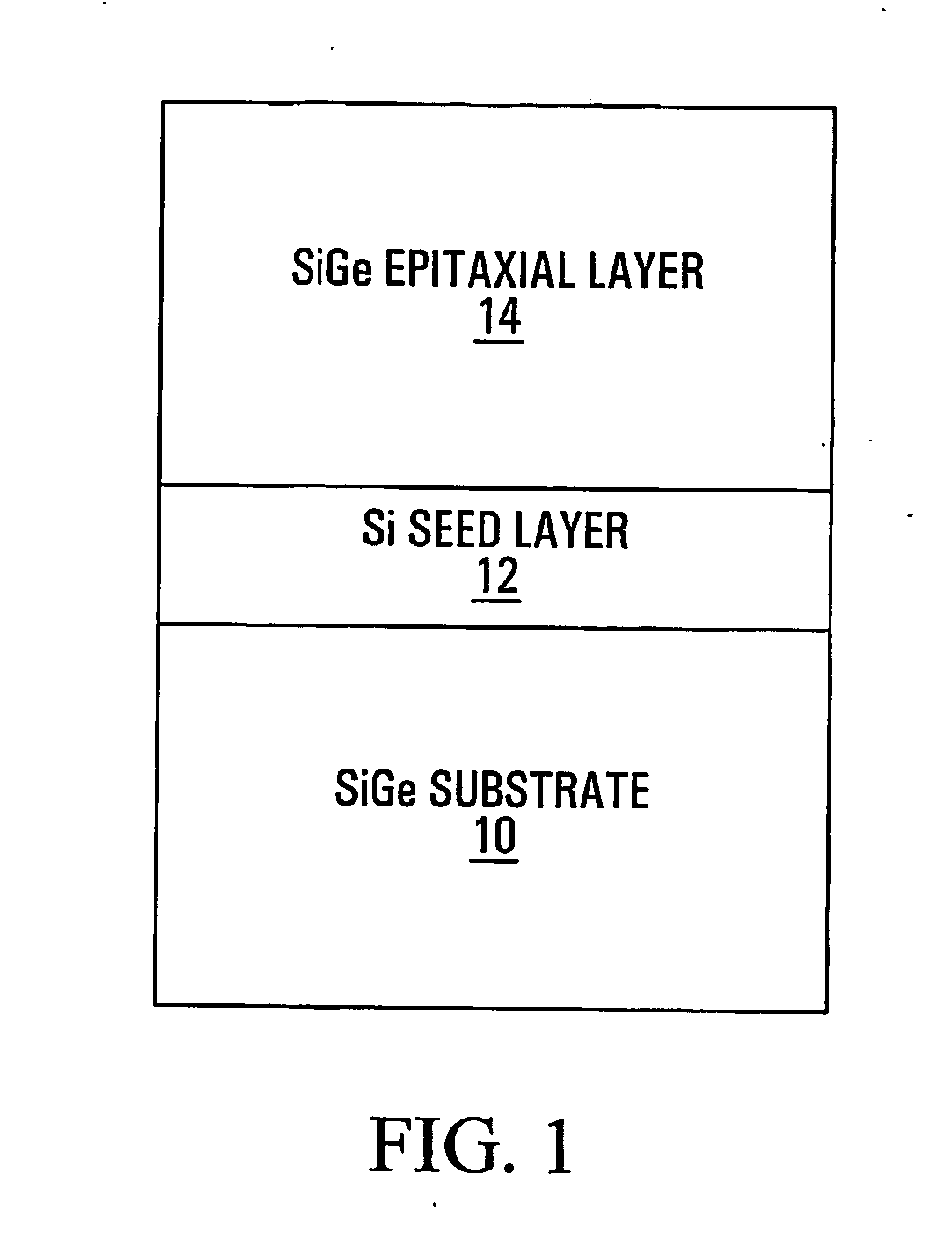
[0020] This invention provides a method of depositing high-quality Si or SiGe epitaxial layers on SiGe substrates. By first depositing a thin Si seed layer on the SiGe substrate, the quality of the seed layer and of the subsequently deposited layers is greatly improved over what is obtained from depositing SiGe directly onto the SiGe substrate. Indeed, whereas the RMS surface roughness of the deposition of SiGe directly on SiGe, as measured by atomic-force microscopy (AFM), was 3-4 nm, it was more than an order of magnitude better when a thin Si seed layer was employed. This work was performed on an ultra-high-vacuum chemical vapor deposition (UHV / CVD) system; however, the same method would apply to other deposition systems such as atmospheric-pressure, low-pressure and rapid-thermal CVD.

[0021] Specifically, referring to FIG. 1, on top of a SiGe substrate 10 there is deposited a thin seed layer 12 of Si and on top of layer 12 there is deposited a layer 12 of SiGe. For the purposes ...


PUM


Abstract

This invention provides a method of depositing high-quality Si or SiGe epitaxial layers on SiGe substrates. By first depositing a thin Si seed layer on the SiGe substrate, the quality of the seed layer and of the subsequently deposited layers is greatly improved over what is obtained from depositing SiGe directly onto the SiGe substrate. Indeed, whereas the RMS surface roughness of the deposition of SiGe directly on SiGe, as measured by atomic-force microscopy (AFM), was 3-4 nm, it was more than an order of magnitude better when a thin Si seed layer was employed. This work was performed on an ultra-high-vacuum chemical vapor deposition (UHV/CVD) system; however, the same method would apply to other deposition systems such as atmospheric-pressure, low-pressure and rapid-thermal CVD.

Description

FIELD OF THE INVENTION [0001] This invention relates to the growth of silicon (Si) or SiGe (Silicon Germanium alloy) epitaxial layers on SiGe substrates. BACKGROUND OF THE INVENTION [0002] The introduction of silicon germanium (SiGe) epitaxial technology has allowed GaAs high-frequency (microwave) transistors to be replaced with silicon transistors in numerous applications. For example, while standard silicon bipolar transistors could not operate reliably above 1 GHz, SiGe Heterostructure Bipolar Transistors (HBT) are now beginning to appear in circuits designed to operate above 10 GHz. [0003] However, SiGe devices fabricated on Silicon (Si) substrates are subject to a number of inherent restrictions. Due to the large lattice mismatch between silicon and germanium (Ge), an alloy SiGe layer grown on top of a silicon substrate or single-crystal surface must remain below a certain critical thickness in order to prevent relaxation through the formation of threading dislocations. Such de...

Claims


Application Information

Patent Timeline
IPC IPC(8): C30B25/02C30B29/52H01L21/20H01L21/205
CPCC30B25/02C30B29/52H01L21/02532H01L21/0245H01L21/02381
Inventor DION, MICHEL MAURICE
Owner SIGE SEMICON
Why Eureka
Try Eureka