Uniform seeding to control grain and defect density of crystallized silicon for use in sub-micron thin film transistors

a thin film transistor and crystallization technology, applied in the direction of transistors, semiconductor devices, electrical equipment, etc., can solve the problems of limiting the use of tfts largely, and not controlling the placement of silicon nuclei

Active Publication Date: 2005-04-07
SANDISK TECH LLC
View PDF11 Cites 40 Cited by
  • Summary
  • Abstract
  • Description
  • Claims
  • Application Information

AI Technical Summary

Problems solved by technology

One of the major obstacles to the use of polysilicon thin film as a semiconductor in active devices is the relatively small grain sizes (around 0.05 micron or less) of polysilicon thin films deposited by such methods as low-pressure chemical vapor deposition and sputtering.
The poor electrical performance caused by grain boundaries in the channel region limits the use of TFTs largely to low-temperature flat panel displays.
In the method of Gu, however, placement of the silicon nuclei is not controlled.
Similarly, if other areas see a lower-than average distribution of silicon nuclei, those areas may require a long anneal time to ensure that no amorphous silicon remains between grains.
The difference in local nucleus densities is one cause of non-uniformity of thin film transistors across a wafer in production.
Placement of seeds at source and drain for every transistor according to Oh et al., while practicable for a single transistor or a small number of transistors, becomes expensive and cumbersome for an array of transistors, particularly when device size is small.
In production this method could become prohibitively expensive due to circuit layout and mask layout changes required for different products and design modifications.

Method used


Image

  • Uniform seeding to control grain and defect density of crystallized silicon for use in sub-micron thin film transistors
  • Uniform seeding to control grain and defect density of crystallized silicon for use in sub-micron thin film transistors
  • Uniform seeding to control grain and defect density of crystallized silicon for use in sub-micron thin film transistors

Examples


first embodiment

[0036] Silicon Nuclei as Crystallizing Agent

[0037] A preferred embodiment which calls for selectively introducing silicon nuclei in a substantially symmetric pattern, where the silicon nuclei behave as a crystallizing agent, will be described in detail.

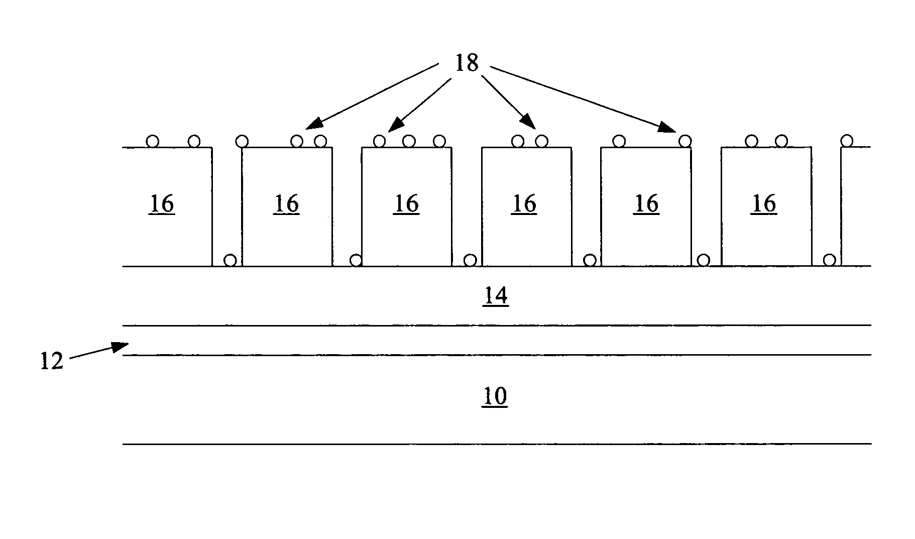
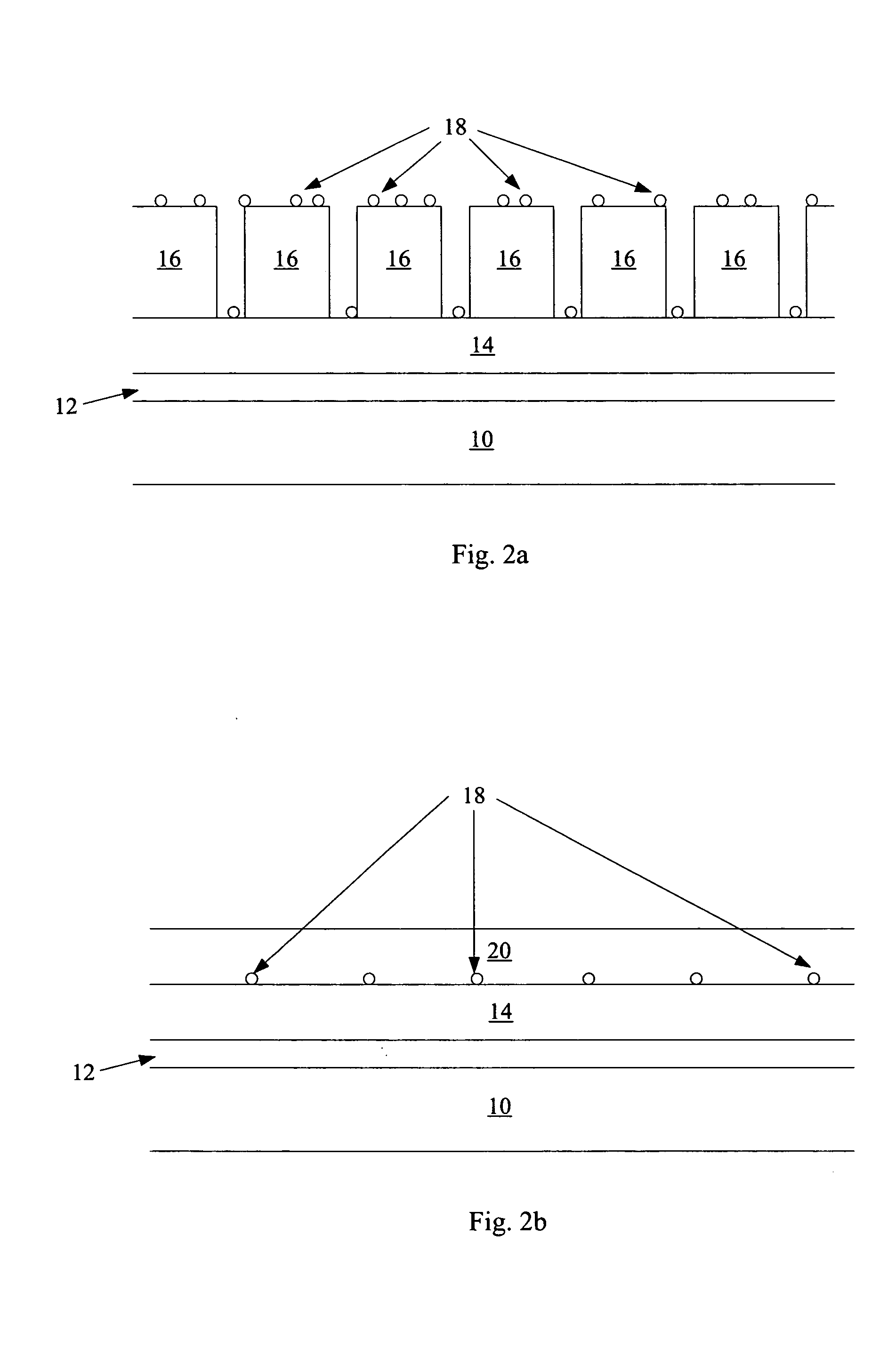
[0038] Deposition of amorphous silicon begins with any suitable substrate. Turning to FIG. 2a, in this example the substrate 10 can be any dielectric or any semiconductive material, such as, for example, a bulk silicon wafer. CMOS or other circuits may be formed in the substrate. A dielectric layer 12 may overlie the substrate 10. Clearly other substrates may be used, and dielectric layer 12 may or may not be present, as may other additional layers.

[0039] Amorphous silicon layer 14, as shown in FIG. 2a, can be deposited by low pressure chemical vapor deposition (LPCVD) or any other method known in the art. Amorphous layer 14 is about 50 to about 1500 angstroms thick, preferably about 500 to about 1000 angstroms thick, more preferab...

second embodiment

[0052] Germanium as Crystallizing Agent

[0053] In some embodiments, germanium is used as a crystallizing agent instead of silicon nuclei. A detailed example will be given, though conditions can be varied and steps can be added or omitted while the method and its results remain within the scope of the invention.

[0054] Turning to FIG. 3, formation of the first amorphous layer 14 over dielectric 12 and, for example, substrate 10, followed by formation, pattern, and etch of holes in mask layer 16 can be done using the same techniques and materials as those described in the previous embodiment, in which the crystallizing agent was silicon nuclei.

[0055] Next a layer of germanium 26 is deposited by any conventional method, for example by LPCVD, for example using GeH4 as a source gas, with temperature of about 500 C at 100 mTorr. Germanium layer 26 is preferably between about 50 and about 200 angstroms thick, more preferably about 100 angstroms thick.

[0056] Under these conditions the dep...

third embodiment

[0059] Laser Energy as Crystallizing Agent

[0060] The crystallizing agent can be laser energy. As in the two previous embodiments, an amorphous silicon layer, for example formed over a dielectric layer and a wafer substrate, is formed using the methods described earlier. This embodiment calls for treating the first amorphous layer with a laser at locations distributed in a substantially symmetric pattern.

[0061] The wafer can be mounted on an x-y linear stage. The wafer surface can be illuminated at substantially uniform intervals. At each point at which the wafer is exposed to laser energy, the amorphous layer is transformed into a large single grain which can grow further upon annealing. The width of the laser and the exposure intervals can be chosen to produce the desired pattern; for example an area 0.5 micron wide can be exposed, with centers of the exposed areas 2 microns apart in a grid pattern.

[0062] The amorphous silicon layer can be irradiated with pulsed (10-100 nsec) Xe...


PUM

PropertyMeasurementUnit
grain sizesaaaaaaaaaa
thickaaaaaaaaaa
thickaaaaaaaaaa

Abstract

A method to create a polysilicon layer with large grains and uniform grain density is described. A first amorphous silicon layer is formed. A crystallizing agent is selectively introduced in a substantially symmetric pattern, preferably symmetric in two dimensions, across an area of the first amorphous layer. The crystallizing agent may be, for example, silicon nuclei, germanium, or laser energy. A mask layer is formed on the amorphous silicon layer, and holes etched in the mask layer in a symmetric pattern to expose the amorphous layer to, for example, silicon nuclei or germanium) only in the holes. The mask layer is removed and a second amorphous layer formed on the first. If laser energy is used, no mask layer or second amorphous layer is generally used. The wafer is annealed to form a polysilicon layer with substantially no amorphous silicon remaining between the grains.

Description

BACKGROUND OF THE INVENTION [0001] The invention relates to a method to enhance grain size in polycrystalline silicon, called polysilicon. Larger grain size in polysilicon is advantageous for many uses, particularly in thin film transistors (TFTs). [0002] One of the major obstacles to the use of polysilicon thin film as a semiconductor in active devices is the relatively small grain sizes (around 0.05 micron or less) of polysilicon thin films deposited by such methods as low-pressure chemical vapor deposition and sputtering. A film with small grain size has a larger number of grain boundaries, decreasing carrier mobility. Typical electron mobilities in polysilicon films made using these methods are on the order of 10 cm2 / volt-second, two orders of magnitude lower than electron mobilities in bulk silicon. [0003] The poor electrical performance caused by grain boundaries in the channel region limits the use of TFTs largely to low-temperature flat panel displays. It is believed that el...

Claims


Application Information

Patent Timeline
Patent Type & Authority Applications(United States)
IPC IPC(8): H01L21/20H01L21/336H01L29/786
CPCH01L21/2022H01L29/78672H01L29/6675H01L21/0262H01L21/02686H01L21/02488H01L21/02532H01L21/02381H01L21/02691H01L21/02675H01L21/02595
Inventor CLEEVES, JAMES M.GU, SHUO
Owner SANDISK TECH LLC
Why Eureka
Try Eureka