Light-emitting device and process for producing thereof

a technology of light-emitting devices and processes, applied in the direction of semiconductor devices, basic electric elements, electrical apparatus, etc., can solve the problems of reducing the unable to sell light-emitting devices, and not being suitable for mass production, so as to improve the effect of removing air bubbles, improving the structural integrity of light-emitting devices, and improving the effect of air bubble removal

Inactive Publication Date: 2005-04-07
NICHIA CORP
View PDF3 Cites 201 Cited by
  • Summary
  • Abstract
  • Description
  • Claims
  • Application Information

AI Technical Summary

Benefits of technology

[0030] Furthermore, it is preferable that the metal base member has a first front surface exposed in the recessed portion, and a second front surface covered in the package to improve the structural integrity of the light-emitting device.
[0031] Furthermore, if a second recessed portion is provided substantially in the center of the front surface of the metal base member exposed in the bottom surface of the recessed portion, arid the light-emitting element is disposed on the bottom surface of the second recessed portion, then outgoing efficiency of light is increased. It can also prevent mixing air bubbles in the flexible member, and further it can improve the effect of removing air bubbles and improve the flowability of the flexible member nearby the light-emitting element. In addition, the second recessed portion can increase the contact area between the flexible member and the metal base member. This increases the length of the path of thermal dissipation so that local deterioration of the flexible member can be prevented.
[0032] It is also preferable that one end portion of each of the pair of lead terminals is exposed from the side surface opposite from the side where one end portion of the metal base member is exposed. It is also preferable to align these end portions in parallel at a predetermined distance apart. This allows the terminals of the mount board to be easily wired. In addition, this allows the light-emitting device to be downsized while maintaining the area of the back surface of the metal base member. Furthermore, the back surface of the package has a notch portion opening at the edge facing the metal base member. It can trap the flow of a conducting member toward the lead terminal by the notch portion. This prevents the electrical flow from reaching the opposite lead terminal, even when the conducting member provided on the back surface of the metal base member is too much. Therefore this arrangement can improve yields.
[0033] Furthermore, in the case where the light-emitting element has a pair of positive and negative terminals in the same side that are preferably coplanar, the pair of terminals is connected by wires. In this arrangement, it would be advantageous that the top points of the wires are positioned between the first front surface and the second front surface. Providing the wires in this position improves flowability of the flexible member, and minimizes the deleterious effects of thermal stress on the wires. In addition, since the lead terminal is provided above each terminal of the light-emitting element, and no impediments exist in the path from the light-emitting element to the lead terminal, wire-bonding can be performed relatively easily with a higher reliability.
[0034] The process for producing a light-emitting device according to the present invention relates to the light-emitting device having a package with a recess portion thereon, in which the light-emitting chip is disposed, a transparent flexible member covering at least the recess portion, a transparent rigid member disposed on or above the flexible member, and a path opening continuously from the bottom surface to the top of the package. This process includes a first step of injecting the transparent flexible member into the recess portion in the package to cover the light-emitting element provided in the recess portion; a second step of pressing the rigid member downwardly to overflow the transparent flexible member over the top surface of the end portion of the transparent rigid member through the path; and a third step of heating to structurally form each member into one body. Consequently, this process produces a light-emitting device with a higher reliability and good optical stability by employing a high yield simplified method.
[0035] In the light-emitting device of the present invention, a light-emitting element is molded with a flexible first covering member and a rigid second member, by providing a continuously open path from the bottom surface to the top of the package which reduces the mixing of air bubbles between the flexible member and the rigid member, and also improves the effect of removing air bubbles mixed in the flexible member.

Problems solved by technology

When the light-emitting chip is molded in place by the flexible member and the rigid member is laminated thereon, air bubbles are prone to be mixed into the flexible member at the interface between them.
The light-emitting device having air bubbles reduces its integrity because of a vapor burst by the air bubbles under high temperature.
Therefore, such light-emitting devices cannot be soldered onto a mount substrate or the like, by a reflow mount and thus they are not appropriate for mass production.
Although the cross-sectional shape of the back surface is adequate to project toward the light-emitting element, it is not specifically so limited.

Method used


Image

  • Light-emitting device and process for producing thereof
  • Light-emitting device and process for producing thereof
  • Light-emitting device and process for producing thereof

Examples


example 1

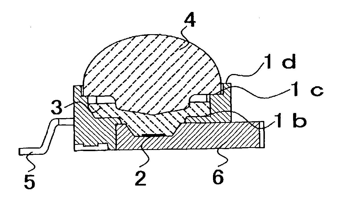
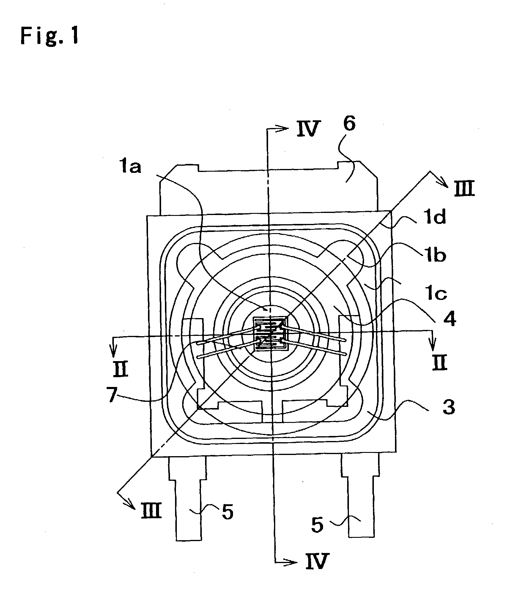
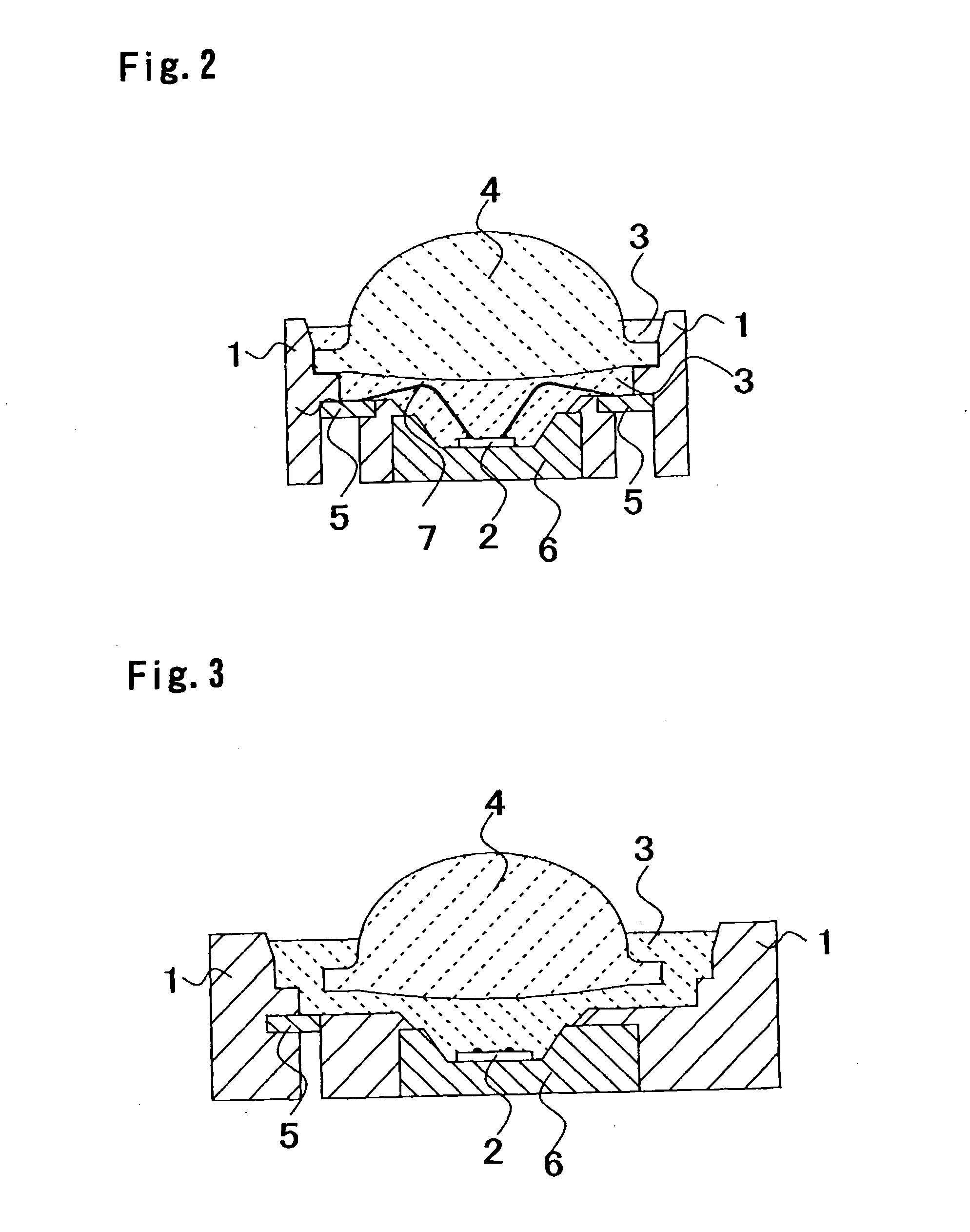
[0128] A surface mount type light-emitting device as shown in FIG. 1 is formed. A nitride semiconductor having a semiconductor of In0.2Ga0.8N with a monochromatic light-emission peak 475 nm as a light-emitting layer is employed as an LED chip. More specifically, the LED chip can be formed by flowing TMG (trimethylgallium) gas, TMT (trimethylindium) gas, nitrogen gas, and a dopant gas with a carrier gas onto a cleaned sapphire substrate so as to laminate nitride semiconductor layers by a MOCVD method. An n-type nitride semiconductor layer and a p-type nitride semiconductor layer can be formed by changing SiH4 and Cp2Mg as the dopant.

[0129] The element structure of the LED chip has an n-type GaN layer, which is an undoped nitride semiconductor, on the sapphire substrate; a GaN layer, which is a Si-doped n-type contact layer providing an n-type terminal thereon; and the light-emitting layer having a multi-quantum-well structure with 5 sets of an InGaN layer successively interposed wit...

example 2

[0137] As shown in FIG. 10, a light-emitting device is formed in the same manner as Example 1 except for forming a cornered outline of the second front surface in a hexagon shape. This provides a light-emitting device with more effective mass production and better mountability with a higher density compared to the device in Example 1.

example 3

[0138] As shown in FIG. 11, a light-emitting device can be formed in the same manner as Example 1 except for 1) forming the outline of the second front surface and the outline of the first front surface in a polygonal shape with similar relations between them, and 2) forming the lens with a notch portion in its outline to expose corners of the first front surface. This structure provides a light-emitting device with effects similar to Example 1.


PUM


Abstract

The light-emitting device includes a light-emitting element chip; a package having a first recessed portion thereon, in which the light-emitting chip is disposed; a transparent flexible member covering at least the recessed portion; and a transparent rigid member disposed on or above the transparent flexible member. The package has at least a first front surface extending at least outwardly above the first recessed portion; a second front surface extending outwardly above the first front surface; and a third surface as the outside of the package extending outwardly above the second front surface. The rigid member is disposed in the outline of the second front surface with at least three points of contact. The flexible member is continuously provided along the first front surface, the second front surface and the back surface of the rigid member. This light-emitting device is capable of improved reliability without deteriorating its optical characteristics.

Description

BACKGROUND OF THE INVENTION [0001] 1. Field of the Invention [0002] The present invention relates to a light-emitting device used for various light sources such as a backlight source, a display, illuminations, etc. or photo sensors, and more specifically to a light-emitting device with higher reliability and preferable optical characteristics. [0003] 2. Discussion of the Related Art [0004] Recently, high-luminance, high-power semiconductor light-emitting elements, or small-scale and high sensitivity light-emitting devices have been developed and used in various fields. Such light-emitting devices have characteristics such as low power consumption, small-scale, lightweight, and therefore they are used as a light source for a light-printer head, a backlight source of liquid crystal display, light sources of various meters, various scanning sensors, etc. [0005]FIG. 23 shows one example of a light-emitting device. A plastic package, which has a recessed portion, formed with integrally i...

Claims


Application Information

Patent Timeline
Patent Type & Authority Applications(United States)
IPC IPC(8): H01L29/22H01L33/48H01L33/52H01L33/54H01L33/58
CPCH01L33/486H01L33/52H01L2224/45144H01L2224/8592H01L2224/73265H01L2224/49111H01L2224/49107H01L2224/48247H01L2224/45139H01L24/45H01L33/54H01L33/58H01L2224/48465H01L2224/45124H01L2924/00014H01L2924/00H01L2924/12042H01L2924/12041H01L2924/181H01L2224/48091H01L2924/00012H01L2224/45015H01L2924/207
Inventor SUENAGA, RYOMA
Owner NICHIA CORP
Why Eureka
Try Eureka